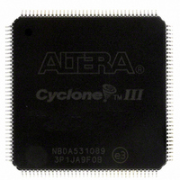
EP3C10E144C8N Altera, EP3C10E144C8N Datasheet - Page 111

EP3C10E144C8N
Manufacturer Part Number
EP3C10E144C8N
Description
IC CYCLONE III FPGA 10K 144-EQFP
Manufacturer
Altera
Series
Cyclone® IIIr
Datasheets
1.EP3C5F256C8N.pdf
(5 pages)
2.EP3C5F256C8N.pdf
(34 pages)
3.EP3C5F256C8N.pdf
(66 pages)
4.EP3C5F256C8N.pdf
(14 pages)
5.EP3C5F256C8N.pdf
(76 pages)
6.EP3C10E144C8N.pdf
(274 pages)
Specifications of EP3C10E144C8N
Number Of Logic Elements/cells
10320
Number Of Labs/clbs
645
Total Ram Bits
423936
Number Of I /o
94
Voltage - Supply
1.15 V ~ 1.25 V
Mounting Type
Surface Mount
Operating Temperature
0°C ~ 85°C
Package / Case
144-EQFP
Family Name
Cyclone III
Number Of Logic Blocks/elements
10320
# I/os (max)
94
Frequency (max)
402MHz
Process Technology
65nm
Operating Supply Voltage (typ)
1.2V
Logic Cells
10320
Ram Bits
423936
Operating Supply Voltage (min)
1.15V
Operating Supply Voltage (max)
1.25V
Operating Temp Range
0C to 85C
Operating Temperature Classification
Commercial
Mounting
Surface Mount
Pin Count
144
Package Type
EQFP
For Use With
544-2601 - KIT DEV CYCLONE III LS EP3CLS200544-2411 - KIT DEV NIOS II CYCLONE III ED.
Lead Free Status / RoHS Status
Lead free / RoHS Compliant
Number Of Gates
-
Lead Free Status / Rohs Status
Compliant
Other names
544-2427
EP3C10E144C8N
EP3C10E144C8N
Available stocks
Company
Part Number
Manufacturer
Quantity
Price
Company:
Part Number:
EP3C10E144C8N
Manufacturer:
ALTERA47
Quantity:
516
Part Number:
EP3C10E144C8N
Manufacturer:
ALTERA
Quantity:
20 000
Chapter 6: I/O Features in the Cyclone III Device Family
I/O Standards
I/O Standards
© December 2009
f
Altera Corporation
Figure 6–5
shown is the intrinsic transistor impedance.
Figure 6–5. Cyclone III Device Family On-Chip Series Termination Without Calibration
All I/O banks and I/O pins support impedance matching and series termination.
Dedicated configuration pins and JTAG pins do not support impedance matching or
series termination.
On-chip series termination is supported on any I/O bank. V
compatible for all I/O pins to enable on-chip series termination in a given I/O bank.
I/O standards that support different R
long as their V
Impedance matching is implemented using the capabilities of the output driver and is
subject to a certain degree of variation, depending on the process, voltage, and
temperature.
For more information about tolerance specification, refer to the
Sheet
The Cyclone III device family supports multiple single-ended and differential I/O
standards. Apart from 3.3-, 3.0-, 2.5-, 1.8-, and 1.5-V support, the Cyclone III device
family also supports 1.2-V I/O standards.
and
Cyclone III LS Device Data Sheet
shows the single-ended I/O standards for OCT without calibration. The R
CCIO
and V
Cyclone III Device Family
Driver Series Termination
REF
are not conflicting.
V
GND
CCIO
R
R
S
S
S
values can reside in the same I/O bank as
chapters.
Z
O
Receiving
Cyclone III Device Handbook, Volume 1
Device
CCIO
Cyclone III Device Data
and V
REF
must be
6–11
S


