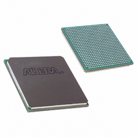
EP1SGX25DF672I6 Altera, EP1SGX25DF672I6 Datasheet - Page 158

EP1SGX25DF672I6
Manufacturer Part Number
EP1SGX25DF672I6
Description
IC STRATIX GX FPGA 25K 672-FBGA
Manufacturer
Altera
Series
Stratix® GXr
Datasheet
1.EP1SGX10CF672C7N.pdf
(272 pages)
Specifications of EP1SGX25DF672I6
Number Of Logic Elements/cells
25660
Number Of Labs/clbs
2566
Total Ram Bits
1944576
Number Of I /o
455
Voltage - Supply
1.425 V ~ 1.575 V
Mounting Type
Surface Mount
Operating Temperature
-40°C ~ 100°C
Package / Case
672-FBGA
Family Name
Stratix GX
Number Of Logic Blocks/elements
25660
# I/os (max)
455
Frequency (max)
5GHz
Process Technology
SRAM
Operating Supply Voltage (typ)
1.5V
Logic Cells
25660
Ram Bits
1944576
Operating Supply Voltage (min)
1.425V
Operating Supply Voltage (max)
1.575V
Operating Temp Range
-40C to 100C
Operating Temperature Classification
Industrial
Mounting
Surface Mount
Pin Count
672
Package Type
FC-FBGA
Lead Free Status / RoHS Status
Contains lead / RoHS non-compliant
Number Of Gates
-
Lead Free Status / Rohs Status
Not Compliant
Available stocks
Company
Part Number
Manufacturer
Quantity
Price
Company:
Part Number:
EP1SGX25DF672I6
Manufacturer:
ALTERA30
Quantity:
50
PLLs & Clock Networks
4–92
Stratix GX Device Handbook, Volume 1
The areset signals are reset/resynchronization inputs for each PLL. The
areset signal should be asserted every time the PLL loses lock to
guarantee correct phase relationship between the PLL output clocks.
Users should include the areset signal in designs if any of the following
conditions are true:
■
■
The device input pins or logic elements (LEs) can drive these input
signals. When driven high, the PLL counters resets, clearing the PLL
output and placing the PLL out of lock. The VCO sets back to its nominal
setting (~700 MHz). When driven low again, the PLL resynchronizes to
its input as it relocks. If the target VCO frequency is below this nominal
frequency, then the output frequency starts at a higher value than desired
as the PLL locks. If the system cannot tolerate this, the clkena signal can
disable the output clocks until the PLL locks.
The pfdena signals control the phase frequency detector (PFD) output
with a programmable gate. If you disable the PFD, the VCO operates at
its last set value of control voltage and frequency with some long-term
drift to a lower frequency. The system continues running when the PLL
goes out of lock or the input clock is disabled. By maintaining the last
locked frequency, the system has time to store its current settings before
shutting down. You can either use your own control signal or a clkloss
status signal to trigger pfdena.
The clkena signals control the enhanced PLL regional and global
outputs. Each regional and global output port has its own clkena signal.
The clkena signals synchronously disable or enable the clock at the PLL
output port by gating the outputs of the g and l counters. The clkena
signals are registered on the falling edge of the counter output clock to
enable or disable the clock without glitches.
waveform example for a PLL clock port enable. The PLL can remain
locked independent of the clkena signals since the loop-related counters
are not affected. This feature is useful for applications that require a low
power or sleep mode. Upon re-enabling, the PLL does not need a
resynchronization or relock period. The clkena signal can also disable
clock outputs if the system is not tolerant to frequency overshoot during
resynchronization.
The extclkena signals work in the same way as the clkena signals, but
they control the external clock output counters (e0, e1, e2, and e3). Upon
re-enabling, the PLL does not need a resynchronization or relock period
PLL Reconfiguration or Clock switchover enables in the design.
Phase relationships between output clocks need to be maintained
after a loss of lock condition
Figure 4–56
Altera Corporation
shows the
February 2005


