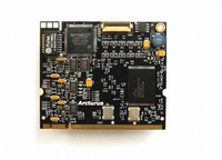
ADSP-3PARCBF548M01 Analog Devices Inc, ADSP-3PARCBF548M01 Datasheet - Page 21

ADSP-3PARCBF548M01
Manufacturer Part Number
ADSP-3PARCBF548M01
Description
MODULE BOARD BF548
Manufacturer
Analog Devices Inc
Series
Blackfin®r
Specifications of ADSP-3PARCBF548M01
Module/board Type
Processor Module
For Use With/related Products
ADSP-BF548
Lead Free Status / RoHS Status
Lead free / RoHS Compliant
• Boot from UART host (BMODE = 0x7)—In this mode, the
• Boot from (DDR) SDRAM (BMODE = 0xA)—In this
• Boot from 8-bit and 16-bit external NAND flash memory
sion 2.1. An I
processor at a time when booting multiple processors from
a single TWI.
processor uses UART1 as the booting source. Using an
autobaud handshake sequence, a boot-stream-formatted
program is downloaded by the host. The host agent selects
a bit rate within the UART’s clocking capabilities.
When performing the autobaud, the UART expects an “@”
(0x40) character (eight data bits, one start bit, one stop bit,
no parity bit) on the UART1RX pin to determine the bit
rate. It then replies with an acknowledgement, which is
composed of four bytes (0xBF, the value of UART1_DLL,
the value of UART1_DLH, and finally 0x00). The host can
then download the boot stream. The processor deasserts
the UART1RTS output to hold off the host; UART1CTS
functionality is not enabled at boot time.
mode, the boot kernel starts booting from address
0x0000 0010. This is a warm boot scenario only. The
SDRAM is expected to contain a valid boot stream and the
SDRAM controller must have been configured by the OTP
settings.
(BMODE = 0xD)—In this mode, auto detection of the
NAND flash device is performed. The processor configures
PORTJ GPIO pins PJ1 and PJ2 to enable the ND_CE and
ND_RB signals, respectively. For correct device operation,
pull-up resistors are required on both ND_CE (PJ1) and
ND_RB (PJ2) signals. By default, a value of 0x0033 is writ-
ten to the NFC_CTL register. The booting procedure
always starts by booting from byte 0 of block 0 of the
NAND flash device. In this boot mode, the HWAIT signal
does not toggle. The respective GPIO pin remains in the
high-impedance state.
NAND flash boot supports the following features:
Small page NAND flash devices must have a 512-byte page
size, 32 pages per block, a 16-byte spare area size and a bus
configuration of eight bits. By default, all read requests
from the NAND flash are followed by four address cycles.
• Device auto detection
• Error detection and correction for maximum
• No boot stream size limitation
• Peripheral DMA via channel 22, providing efficient
• Software-configurable boot mode for booting from
• Software-configurable boot mode for booting from
• Configurable timing via OTP memory
reliability
transfer of all data (excluding the ECC parity data)
boot streams expanding multiple blocks, including
bad blocks
multiple copies of the boot stream allowing for han-
dling of bad blocks and uncorrectable errors
2
C multiplexer can be used to select one
ADSP-BF542/ADSP-BF544/ADSP-BF547/ADSP-BF548/ADSP-BF549
Rev. C | Page 21 of 100 | February 2010
Table 10. Byte 4 Electronic Signature Specification
Large page devices must support the following command set:
Large page devices must not support or react to NAND flash
command 0x50. This is a small page NAND flash command
used for device auto detection.
If the NAND flash device requires only three address
cycles, then the device must be capable of ignoring the
additional address cycle.
The small page NAND flash device must comply with the
following command set:
For large page NAND flash devices, the 4-byte electronic
signature is read in order to configure the kernel for boot-
ing. This allows support for multiple large page devices.
The fourth byte of the electronic signature must comply
with the specifications in
Any configuration from
the command set listed below is directly supported by the
boot kernel. There are no restrictions on the page size or
block size as imposed by the small-page boot kernel.
Page Size
(excluding spare
area)
Spare Area Size
Block Size
(excluding spare
area)
Bus Width
Not Used for
Configuration
Reset: 0xFF
Read lower half of page: 0x00
Read upper half of page: 0x01
Read spare area: 0x50
Reset: 0xFF
Read Electronic Signature: 0x90
Read: 0x00, 0x30 (confirm command)
D1:D0
D2
D5:4
D6
D3, D7
Table 10
Table
00
01
10
11
0
1
00
01
10
11
0
1
10.
that also complies with
1K bytes
2K bytes
4K bytes
8K bytes
8 bytes/512 bytes
16 bytes/512 bytes
64K bytes
128K bytes
256K bytes
512K bytes
x8
x16


