ADSP-3PARCBF548M01 Analog Devices Inc, ADSP-3PARCBF548M01 Datasheet - Page 26
ADSP-3PARCBF548M01
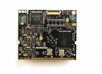
Manufacturer Part Number
ADSP-3PARCBF548M01
Description
MODULE BOARD BF548
Manufacturer
Analog Devices Inc
Series
Blackfin®r
Specifications of ADSP-3PARCBF548M01
Module/board Type
Processor Module
For Use With/related Products
ADSP-BF548
Lead Free Status / RoHS Status
Lead free / RoHS Compliant


ADSP-BF542/ADSP-BF544/ADSP-BF547/ADSP-BF548/ADSP-BF549
Table 11. Pin Multiplexing (Continued)
1
2
3
4
ADSP-BF54x processor pin definitions are listed in
see the pin multiplexing scheme, see
Table 12. Pin Descriptions
Primary Pin
Function
(Number of
Pins)
Port H
GPIO (14 pins)
Port I
GPIO (16 pins)
Port J
GPIO (14 pins)
Pin Name
Port A: GPIO/SPORT2–3/TMR4–7
PA0/TFS2
PA1/DT2SEC/TMR4
PA2/DT2PRI
PA3/TSCLK2
PA4/RFS2
PA5/DR2SEC/TMR5
PA6/DR2PRI
PA7/RSCLK2/TACLK0
PA8/TFS3/TACLK1
PA9/DT3SEC/TMR6
PA10/DT3PRI/TACLK2
PA11/TSCLK3/TACLK3
PA12/RFS3/TACLK4
PA13/DR3SEC/TMR7/TACLK5
PA14/DR3PRI/TACLK6
PA15/RSCLK3/TACLK7 and TACI7
Port connections may be inputs or outputs after power up depending on the model and boot mode chosen.
All port connections always power up as inputs for some period of time and require resistive termination to a safe condition if used as outputs in the system.
A total of 32 interrupts at once are available from ports C through J, configurable in byte-wide blocks.
GPW functionality available when MXVR is not present or unused.
1, 2
First Peripheral
Function
UART1 (2 pins)
ATAPI_RESET (1 pin)
HOST_ADDR (1 pin)
HOST_ACK (1 pin)
MXVR MRX, MTX,
MRXON/GPW
(3 pins)
Async Addr10–25
(16 pins)
Async CTL and MISC
4
Table
11.
Second Peripheral
Function
PPI0-1_FS3 (2 pins)
TMR8 (1 pin)
TMR9 (1 pin)
TMR10 (1 pin)
AMC Addr 4-9 (6 pins)
Rev. C | Page 26 of 100 | February 2010
Table
I/O
I/O GPIO/SPORT2 Transmit Frame Sync
I/O GPIO/SPORT2 Transmit Data Secondary/Timer 4
I/O GPIO/SPORT2 Transmit Data Primary
I/O GPIO/SPORT2 Transmit Serial Clock
I/O GPIO/SPORT2 Receive Frame Sync
I/O GPIO/SPORT2 Receive Data Secondary/Timer 5
I/O GPIO/SPORT2 Receive Data Primary
I/O GPIO/SPORT2 Receive Serial Clock/Alternate Input Clock 0
I/O GPIO/SPORT3 Transmit Frame Sync/Alternate Input Clock 1
I/O GPIO/SPORT3 Transmit Data Secondary/Timer 6
I/O GPIO/SPORT3 Transmit Data Primary/Alternate Input Clock 2
I/O GPIO/SPORT3 Transmit Serial Clock/Alternate Input Clock 3
I/O GPIO/SPORT3 Receive Frame Sync/Alternate Input Clock 4
I/O GPIO/SPORT3 Receive Data Secondary/Timer 7/Alternate Input Clock 5
I/O GPIO/SPORT3 Receive Data Primary/Alternate Input Clock 6
I/O GPIO/SPORT3 Receive Serial Clock/Alt Input Clock 7 and Alt Capture Input 7 A
1
12. To
Function (First/Second/Third/Fourth)
Third Peripheral
Function
TACI1 (1 pin)
Counter Down/Gate
Counter Up/Dir
DMAR 0–1 (2 pins)
PPI2_FS3 (1 pin)
(1 pin)
(1 pin)
Fourth Peripheral
Function
TACI8–10 (3 pins)
TACLK8–10 (3 pins)
HWAITA
Interrupt Capability
Interrupts (8 pins)
Interrupts (6 pins)
Interrupts (8 pins)
Interrupts (8 pins)
Interrupts (8 pins)
Interrupts (6 pins)
C
A
C
C
C
A
C
Driver
Type
C
C
C
A
C
C
C
C
2
Related parts for ADSP-3PARCBF548M01
Image
Part Number
Description
Manufacturer
Datasheet
Request
R

Part Number:
Description:
±1.7g Dual-Axis IMEMS Accelerometer Evaluation Board
Manufacturer:
Analog Devices Inc
Datasheet:

Part Number:
Description:
Inertial Sensor Evaluation System
Manufacturer:
Analog Devices Inc
Datasheet:
Part Number:
Description:
Manufacturer:
Analog Devices Inc
Datasheet:
Part Number:
Description:
Manufacturer:
Analog Devices Inc
Datasheet:
Part Number:
Description:
Manufacturer:
Analog Devices Inc
Datasheet:
Part Number:
Description:
Manufacturer:
Analog Devices Inc
Datasheet:
Part Number:
Description:
Manufacturer:
Analog Devices Inc
Datasheet:
Part Number:
Description:
Manufacturer:
Analog Devices Inc
Datasheet:
Part Number:
Description:
Manufacturer:
Analog Devices Inc
Datasheet:
Part Number:
Description:
Manufacturer:
Analog Devices Inc
Datasheet:
Part Number:
Description:
Manufacturer:
Analog Devices Inc
Datasheet:
Part Number:
Description:
Manufacturer:
Analog Devices Inc
Datasheet:
Part Number:
Description:
Manufacturer:
Analog Devices Inc
Datasheet: