ADSP-3PARCBF548M01 Analog Devices Inc, ADSP-3PARCBF548M01 Datasheet - Page 24
ADSP-3PARCBF548M01
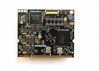
Manufacturer Part Number
ADSP-3PARCBF548M01
Description
MODULE BOARD BF548
Manufacturer
Analog Devices Inc
Series
Blackfin®r
Specifications of ADSP-3PARCBF548M01
Module/board Type
Processor Module
For Use With/related Products
ADSP-BF548
Lead Free Status / RoHS Status
Lead free / RoHS Compliant


ADSP-BF542/ADSP-BF544/ADSP-BF547/ADSP-BF548/ADSP-BF549
Fiber optic transceiver (FOT) connections:
RELATED DOCUMENTS
The following publications that describe the ADSP-BF54x
Blackfin processors (and related processors) can be ordered
from any Analog Devices sales office or accessed electronically
on www.analog.com:
LOCKBOX SECURE TECHNOLOGY DISCLAIMER
Analog Devices products containing Lockbox Secure Technol-
ogy are warranted by Analog Devices as detailed in the Analog
Devices Standard Terms and Conditions of Sale. To our knowl-
edge, the Lockbox secure technology, when used in accordance
with the data sheet and hardware reference manual specifica-
tions, provides a secure method of implementing code and data
safeguards. However, Analog Devices does not guarantee that
this technology provides absolute security. ACCORDINGLY,
ANALOG DEVICES HEREBY DISCLAIMS ANY AND ALL
EXPRESS AND IMPLIED WARRANTIES THAT THE LOCK-
BOX SECURE TECHNOLOGY CANNOT BE BREACHED,
COMPROMISED, OR OTHERWISE CIRCUMVENTED AND
IN NO EVENT SHALL ANALOG DEVICES BE LIABLE FOR
ANY LOSS, DAMAGE, DESTRUCTION, OR RELEASE OF
DATA, INFORMATION, PHYSICAL PROPERTY, OR INTEL-
LECTUAL PROPERTY.
• Keep the traces between the ADSP-BF549 processor and
• The receive data trace connecting the FOT receive data
• The transmit data trace connecting the ADSP-BF549
• The receive data trace and the transmit data trace between
• ADSP-BF54x Blackfin Processor Hardware Reference, Vol-
• Blackfin Processor Programming Reference
• ADSP-BF542/BF544/BF547/BF548/BF549
the FOT as short as possible.
output pin to the ADSP-BF549 PH6/MRX input pin should
have a 0 Ω series termination resistor placed close to the
FOT receive data output pin. Typically, the edge rate of the
FOT receive data signal driven by the FOT is very slow, and
further degradation of the edge rate is not desirable.
PH5/MTX output pin to the FOT transmit data input pin
should have a 27 Ω series termination resistor placed close
to the ADSP-BF549 PH5/MTX pin.
the ADSP-BF549 processor and the FOT should not be
routed close to each other in parallel over long distances to
avoid crosstalk.
ume 1 and Volume 2
Blackfin Anomaly List
Rev. C | Page 24 of 100 | February 2010
Related parts for ADSP-3PARCBF548M01
Image
Part Number
Description
Manufacturer
Datasheet
Request
R

Part Number:
Description:
±1.7g Dual-Axis IMEMS Accelerometer Evaluation Board
Manufacturer:
Analog Devices Inc
Datasheet:

Part Number:
Description:
Inertial Sensor Evaluation System
Manufacturer:
Analog Devices Inc
Datasheet:
Part Number:
Description:
Manufacturer:
Analog Devices Inc
Datasheet:
Part Number:
Description:
Manufacturer:
Analog Devices Inc
Datasheet:
Part Number:
Description:
Manufacturer:
Analog Devices Inc
Datasheet:
Part Number:
Description:
Manufacturer:
Analog Devices Inc
Datasheet:
Part Number:
Description:
Manufacturer:
Analog Devices Inc
Datasheet:
Part Number:
Description:
Manufacturer:
Analog Devices Inc
Datasheet:
Part Number:
Description:
Manufacturer:
Analog Devices Inc
Datasheet:
Part Number:
Description:
Manufacturer:
Analog Devices Inc
Datasheet:
Part Number:
Description:
Manufacturer:
Analog Devices Inc
Datasheet:
Part Number:
Description:
Manufacturer:
Analog Devices Inc
Datasheet:
Part Number:
Description:
Manufacturer:
Analog Devices Inc
Datasheet: