ADSP-3PARCBF548M01 Analog Devices Inc, ADSP-3PARCBF548M01 Datasheet - Page 46
ADSP-3PARCBF548M01
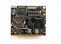
Manufacturer Part Number
ADSP-3PARCBF548M01
Description
MODULE BOARD BF548
Manufacturer
Analog Devices Inc
Series
Blackfin®r
Specifications of ADSP-3PARCBF548M01
Module/board Type
Processor Module
For Use With/related Products
ADSP-BF548
Lead Free Status / RoHS Status
Lead free / RoHS Compliant


ADSP-BF542/ADSP-BF544/ADSP-BF547/ADSP-BF548/ADSP-BF549
Asynchronous Memory Write Cycle Timing
Table 30
on Page 47
tions for synchronous and for asynchronous ARDY.
Table 30. Asynchronous Memory Write Cycle Timing with Synchronous ARDY
1
Parameter
Timing Requirements
t
t
Switching Characteristics
t
t
t
t
Output pins include AMS3–0, ABE1–0, ADDR19–1, and AWE.
SARDY
HARDY
DDAT
ENDAT
DO
HO
and
describe asynchronous memory write cycle opera-
Table 31 on Page 47
ARDY Setup Before the Falling Edge of CLKOUT
ARDY Hold After the Falling Edge of CLKOUT
DATA15–0 Disable After CLKOUT
DATA15–0 Enable After CLKOUT
Output Delay After CLKOUT
Output Hold After CLKOUT
DATA 15–0
ADDR19–1
CLKOUT
ABE1–0
AMSx
ARDY
and
AWE
Figure 15. Asynchronous Memory Write Cycle Timing with Synchronous ARDY
t
ENDAT
Figure 15
1
t
1
DO
2 CYCLES
and
SETUP
Rev. C | Page 46 of 100 | February 2010
Figure 16
t
SARDY
t
WRITE ACCESS
DO
PROGRAMMED
2 CYCLES
t
SARDY
t
HARDY
ACCESS
1 CYCLE
EXTEND
t
HARDY
1 CYCLE
t
HO
HOLD
t
HO
t
DDAT
Min
5.0
0.0
0.0
0.3
Max
6.0
6.0
Unit
ns
ns
ns
ns
ns
ns
Related parts for ADSP-3PARCBF548M01
Image
Part Number
Description
Manufacturer
Datasheet
Request
R

Part Number:
Description:
±1.7g Dual-Axis IMEMS Accelerometer Evaluation Board
Manufacturer:
Analog Devices Inc
Datasheet:

Part Number:
Description:
Inertial Sensor Evaluation System
Manufacturer:
Analog Devices Inc
Datasheet:
Part Number:
Description:
Manufacturer:
Analog Devices Inc
Datasheet:
Part Number:
Description:
Manufacturer:
Analog Devices Inc
Datasheet:
Part Number:
Description:
Manufacturer:
Analog Devices Inc
Datasheet:
Part Number:
Description:
Manufacturer:
Analog Devices Inc
Datasheet:
Part Number:
Description:
Manufacturer:
Analog Devices Inc
Datasheet:
Part Number:
Description:
Manufacturer:
Analog Devices Inc
Datasheet:
Part Number:
Description:
Manufacturer:
Analog Devices Inc
Datasheet:
Part Number:
Description:
Manufacturer:
Analog Devices Inc
Datasheet:
Part Number:
Description:
Manufacturer:
Analog Devices Inc
Datasheet:
Part Number:
Description:
Manufacturer:
Analog Devices Inc
Datasheet:
Part Number:
Description:
Manufacturer:
Analog Devices Inc
Datasheet: