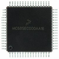
MC68SEC000AA16 Freescale Semiconductor, MC68SEC000AA16 Datasheet - Page 27

MC68SEC000AA16
Manufacturer Part Number
MC68SEC000AA16
Description
IC MPU 32BIT 16MHZ 64-QFP
Manufacturer
Freescale Semiconductor
Series
M68000r
Specifications of MC68SEC000AA16
Processor Type
M680x0 32-Bit
Speed
16MHz
Voltage
3.3V, 5V
Mounting Type
Surface Mount
Package / Case
64-QFP
Processor Series
M680xx
Core
CPU32
Maximum Clock Frequency
16 MHz
Operating Supply Voltage
3.3 V, 5 V
Maximum Operating Temperature
+ 105 C
Mounting Style
SMD/SMT
Minimum Operating Temperature
0 C
Core Size
32 Bit
Cpu Speed
16MHz
Digital Ic Case Style
QFP
No. Of Pins
64
Supply Voltage Range
5V
Operating Temperature Range
0°C To +70°C
Frequency Typ
20MHz
Filter Terminals
SMD
Rohs Compliant
Yes
Clock Frequency
16MHz
Lead Free Status / RoHS Status
Lead free / RoHS Compliant
Features
-
Lead Free Status / Rohs Status
Lead free / RoHS Compliant
Available stocks
Company
Part Number
Manufacturer
Quantity
Price
Company:
Part Number:
MC68SEC000AA16
Manufacturer:
Freescale Semiconductor
Quantity:
10 000
Part Number:
MC68SEC000AA16
Manufacturer:
FREESCALE
Quantity:
20 000
Company:
Part Number:
MC68SEC000AA16R2
Manufacturer:
Freescale Semiconductor
Quantity:
10 000
PA6–PA4 serve as either general-purpose outputs, timer input captures, or timer output compare 2–4. In
addition, PA6–PA4 can be controlled by OC1.
PA3 can be a general-purpose I/O pin or a timer IC/OC pin. Timer functions associated with this pin
include OC1 and IC4/OC5. IC4/OC5 is software selectable as either a fourth input capture or a fifth output
compare. PA3 can also be configured to allow OC1 edges to trigger IC4 captures.
PA2–PA0 serve as general-purpose inputs or as IC1–IC3.
PORTA can be read at any time. Reads of pins configured as inputs return the logic level present on the
pin. Pins configured as outputs return the logic level present at the pin driver input. If written, PORTA
stores the data in an internal latch, bits 7 and 3. It drives the pins only if they are configured as outputs.
Writes to PORTA do not change the pin state when pins are configured for timer input captures or output
compares. Refer to
1.4.13 Port B
During single-chip operating modes, all port B pins are general-purpose output pins. During MCU reads
of this port, the level sensed at the input side of the port B output drivers is read. Port B can also be used
in simple strobed output mode. In this mode, an output pulse appears at the STRB signal each time data
is written to port B.
In expanded multiplexed operating modes, all of the port B pins act as high order address output signals.
During each MCU cycle, bits 15–8 of the address bus are output on the PB7–PB0 pins. The PORTB
register is treated as an external address in expanded modes.
1.4.14 Port C
While in single-chip operating modes, all port C pins are general-purpose I/O pins. Port C inputs can be
latched into an alternate PORTCL register by providing an input transition to the STRA signal. Port C can
also be used in full handshake modes of parallel I/O where the STRA input and STRB output act as
handshake control lines.
When in expanded multiplexed modes, all port C pins are configured as multiplexed address/data signals.
During the address portion of each MCU cycle, bits 7–0 of the address are output on the PC7–PC0 pins.
During the data portion of each MCU cycle (E high), PC7–PC0 are bidirectional data signals,
DATA7–DATA0. The direction of data at the port C pins is indicated by the R/W signal.
The CWOM control bit in the PIOC register disables the port C P-channel output driver. CWOM
simultaneously affects all eight bits of port C. Because the N-channel driver is not affected by CWOM,
setting CWOM causes port C to become an open-drain type output port suitable for wired-OR operation.
In wired-OR mode:
It is customary to have an external pullup resistor on lines that are driven by open-drain devices. Port C
can only be configured for wired-OR operation when the MCU is in single-chip mode. Refer to
Freescale Semiconductor
Parallel Input/Output (I/O) Ports
•
•
When a port C bit is at logic level 0, it is driven low by the N-channel driver.
When a port C bit is at logic level 1, the associated pin has high-impedance, as neither the
N-channel nor the P-channel devices are active.
Chapter 6 Parallel Input/Output (I/O)
for additional information about port C functions.
M68HC11E Family Data Sheet, Rev. 5.1
Ports.
Pin Descriptions
Chapter 6
27


