MC68SEC000AA16 Freescale Semiconductor, MC68SEC000AA16 Datasheet - Page 84
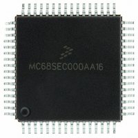
MC68SEC000AA16
Manufacturer Part Number
MC68SEC000AA16
Description
IC MPU 32BIT 16MHZ 64-QFP
Manufacturer
Freescale Semiconductor
Series
M68000r
Specifications of MC68SEC000AA16
Processor Type
M680x0 32-Bit
Speed
16MHz
Voltage
3.3V, 5V
Mounting Type
Surface Mount
Package / Case
64-QFP
Processor Series
M680xx
Core
CPU32
Maximum Clock Frequency
16 MHz
Operating Supply Voltage
3.3 V, 5 V
Maximum Operating Temperature
+ 105 C
Mounting Style
SMD/SMT
Minimum Operating Temperature
0 C
Core Size
32 Bit
Cpu Speed
16MHz
Digital Ic Case Style
QFP
No. Of Pins
64
Supply Voltage Range
5V
Operating Temperature Range
0°C To +70°C
Frequency Typ
20MHz
Filter Terminals
SMD
Rohs Compliant
Yes
Clock Frequency
16MHz
Lead Free Status / RoHS Status
Lead free / RoHS Compliant
Features
-
Lead Free Status / Rohs Status
Lead free / RoHS Compliant
Available stocks
Company
Part Number
Manufacturer
Quantity
Price
Company:

Part Number:
MC68SEC000AA16
Manufacturer:
Freescale Semiconductor
Quantity:
10 000
Part Number:
MC68SEC000AA16
Manufacturer:
FREESCALE
Quantity:
20 000
Company:
Part Number:
MC68SEC000AA16R2
Manufacturer:
Freescale Semiconductor
Quantity:
10 000


Resets and Interrupts
5.3.2 Memory Map
After reset, the INIT register is initialized to $01, mapping the RAM at $00 and the control registers at
$1000.
For the MC68HC811E2, the CONFIG register resets to $FF. EEPROM mapping bits (EE[3:0]) place the
EEPROM at $F800. Refer to the memory map diagram for MC68HC811E2 in
Chapter 2 Operating Modes
and On-Chip
Memory.
5.3.3 Timer
During reset, the timer system is initialized to a count of $0000. The prescaler bits are cleared, and all
output compare registers are initialized to $FFFF. All input capture registers are indeterminate after reset.
The output compare 1 mask (OC1M) register is cleared so that successful OC1 compares do not affect
any I/O pins. The other four output compares are configured so that they do not affect any I/O pins on
successful compares. All input capture edge-detector circuits are configured for capture disabled
operation. The timer overflow interrupt flag and all eight timer function interrupt flags are cleared. All nine
timer interrupts are disabled because their mask bits have been cleared.
The I4/O5 bit in the PACTL register is cleared to configure the I4/O5 function as OC5; however, the
OM5:OL5 control bits in the TCTL1 register are clear so OC5 does not control the PA3 pin.
5.3.4 Real-Time Interrupt (RTI)
The real-time interrupt flag (RTIF) is cleared and automatic hardware interrupts are masked. The rate
control bits are cleared after reset and can be initialized by software before the real-time interrupt (RTI)
system is used.
5.3.5 Pulse Accumulator
The pulse accumulator system is disabled at reset so that the pulse accumulator input (PAI) pin defaults
to being a general-purpose input pin.
5.3.6 Computer Operating Properly (COP)
The COP watchdog system is enabled if the NOCOP control bit in the CONFIG register is cleared and
disabled if NOCOP is set. The COP rate is set for the shortest duration timeout.
5.3.7 Serial Communications Interface (SCI)
The reset condition of the SCI system is independent of the operating mode. At reset, the SCI baud rate
control register (BAUD) is initialized to $04. All transmit and receive interrupts are masked and both the
transmitter and receiver are disabled so the port pins default to being general-purpose I/O lines. The SCI
frame format is initialized to an 8-bit character size. The send break and receiver wakeup functions are
disabled. The TDRE and TC status bits in the SCI status register (SCSR) are both 1s, indicating that there
is no transmit data in either the transmit data register or the transmit serial shift register. The RDRF, IDLE,
OR, NF, FE, PF, and RAF receive-related status bits in the SCI control register 2 (SCCR2) are cleared.
5.3.8 Serial Peripheral Interface (SPI)
The SPI system is disabled by reset. The port pins associated with this function default to being
general-purpose I/O lines.
M68HC11E Family Data Sheet, Rev. 5.1
84
Freescale Semiconductor
Related parts for MC68SEC000AA16
Image
Part Number
Description
Manufacturer
Datasheet
Request
R

Part Number:
Description:
Manufacturer:
Freescale Semiconductor, Inc
Datasheet:
Part Number:
Description:
Manufacturer:
Freescale Semiconductor, Inc
Datasheet:
Part Number:
Description:
Manufacturer:
Freescale Semiconductor, Inc
Datasheet:
Part Number:
Description:
Manufacturer:
Freescale Semiconductor, Inc
Datasheet:
Part Number:
Description:
Manufacturer:
Freescale Semiconductor, Inc
Datasheet:
Part Number:
Description:
Manufacturer:
Freescale Semiconductor, Inc
Datasheet:
Part Number:
Description:
Manufacturer:
Freescale Semiconductor, Inc
Datasheet:
Part Number:
Description:
Manufacturer:
Freescale Semiconductor, Inc
Datasheet:
Part Number:
Description:
Manufacturer:
Freescale Semiconductor, Inc
Datasheet:
Part Number:
Description:
Manufacturer:
Freescale Semiconductor, Inc
Datasheet:
Part Number:
Description:
Manufacturer:
Freescale Semiconductor, Inc
Datasheet:
Part Number:
Description:
Manufacturer:
Freescale Semiconductor, Inc
Datasheet:
Part Number:
Description:
Manufacturer:
Freescale Semiconductor, Inc
Datasheet:
Part Number:
Description:
Manufacturer:
Freescale Semiconductor, Inc
Datasheet:
Part Number:
Description:
Manufacturer:
Freescale Semiconductor, Inc
Datasheet: