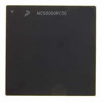
MC68060RC50 Freescale Semiconductor, MC68060RC50 Datasheet - Page 191

MC68060RC50
Manufacturer Part Number
MC68060RC50
Description
IC MPU 32BIT 50MHZ 206-PGA
Manufacturer
Freescale Semiconductor
Specifications of MC68060RC50
Processor Type
M680x0 32-Bit
Speed
50MHz
Voltage
3.3V
Mounting Type
Surface Mount
Package / Case
206-PGA
Family Name
M68000
Device Core
ColdFire
Device Core Size
32b
Frequency (max)
50MHz
Instruction Set Architecture
RISC
Supply Voltage 1 (typ)
3.3V
Operating Supply Voltage (max)
3.465V
Operating Supply Voltage (min)
3.135V
Operating Temp Range
0C to 110C
Operating Temperature Classification
Commercial
Mounting
Through Hole
Pin Count
206
Package Type
PGA
Lead Free Status / RoHS Status
Contains lead / RoHS non-compliant
Features
-
Lead Free Status / Rohs Status
Compliant
Available stocks
Company
Part Number
Manufacturer
Quantity
Price
Company:
Part Number:
MC68060RC50
Manufacturer:
MOTO
Quantity:
5 530
Company:
Part Number:
MC68060RC50C
Manufacturer:
MOTO
Quantity:
5 530
Company:
Part Number:
MC68060RC50C
Manufacturer:
MOTO
Quantity:
5 530
Company:
Part Number:
MC68060RC50C
Manufacturer:
SAMSUNG
Quantity:
5 704
- Current page: 191 of 416
- Download datasheet (2Mb)
Bus Operation
and if TA and TEA are both asserted, the processor retries the cycle. If operating in native-
MC68060 acknowledge termination mode, a retry is indicated by the assertion of TRA.
Note that the acknowledge termination ignore state capability is applicable to the interrupt
acknowledge cycle. If enabled, TA, TEA, TRA, and other acknowledge termination signals
are ignored for a user-programmed number of BCLK cycles.
7.8.2 Breakpoint Acknowledge Cycle
The execution of a BKPT instruction generates the breakpoint acknowledge cycle. An
acknowledged access is a read bus cycle and is indicated with TT1, TT0 = $3, address A31–
A0 = $00000000, and TM2–TM0 = $0. When the external device terminates the cycle with
either TA or TEA, the processor takes an illegal instruction exception. A retry termination
simply retries the breakpoint acknowledge cycle. Figure 7-30 and Figure 7-31 illustrate a
flowchart and functional timing diagram for a breakpoint acknowledge bus cycle.
7-36
10) DRIVE SIZ1–SIZ0 TO BYTE
11) ASSERT TS FOR ONE BCLK
12) ASSERT TIP
13) ASSERT SAS IMMEDIATELY IF
1) IPEND RECOGNIZED. WAIT FOR INSTRUC-
2) SET R/W TO READ
3) DRIVE ADDRESS ON A31–A0 TO $FFFFFFFF
4) DRIVE UPA1–UPA0 = 0
5) DRIVE TT1–TT0 = 3
6) DRIVE TM2–TM0 = INTERRUPT LEVEL
7) DRIVE TLN1–TLN0 = 0
8) ASSERT BS3
9) NEGATIVE CIOUT, LOCK, LOCKE, BS2–BS0
1) IF NORMAL TERMINATION (TA ONLY) WITH
2) IF NORMAL TERMINATION (TA ONLY) WITH
3) IF BUS ERROR TERMINATION, USE VEC-
4) IF RETRY TERMINATION, RETRY IACK
1) NEGATE TIP OR START NEXT CYCLE
AVEC ASSERTED, USE VECTORS 25 TO 31,
DEPANDING ON INTERRUPT LEVEL
AVEC NEGATED, USE VECTOR GIVEN IN
D7–D0
TOR 24
CYCLE
TION BOUNDARY OR LOCK NEGATED
ACKNOWLEDGE TERMINATION IGNORE
STATE CAPABILITY DISABLED. ELSE,
ASSERT SAS AFTER READ PRIMARY
IGNORE STATE COUNTER HAS EXPIRED
Figure 7-27. Interrupt Acknowledge Cycle Flowchart
M68060 USER’S MANUAL
1) ASSERT IPL2–IPL0 SUCH THAT INTERRUPT
1) DECODE ADDRESS AND ATTRIBUTES
2) EITHER PLACE VECTOR ON D7–D0 OR
3) ASSERT TA, TEA, OR TRA FOR ONE BCLK
1) THREE-STATE D31–D0
2) NEGATE AVEC IF NECESSARY
LEVEL GREATER THAN MASK LEVEL IN SR
ASSERT AVEC
MOTOROLA
Related parts for MC68060RC50
Image
Part Number
Description
Manufacturer
Datasheet
Request
R
Part Number:
Description:
Mc68060 Superscalar 68k Microprocessor Including The Lc060 And Ec060
Manufacturer:
Freescale Semiconductor, Inc
Datasheet:
Part Number:
Description:
Manufacturer:
Freescale Semiconductor, Inc
Datasheet:
Part Number:
Description:
Manufacturer:
Freescale Semiconductor, Inc
Datasheet:
Part Number:
Description:
Manufacturer:
Freescale Semiconductor, Inc
Datasheet:
Part Number:
Description:
Manufacturer:
Freescale Semiconductor, Inc
Datasheet:
Part Number:
Description:
Manufacturer:
Freescale Semiconductor, Inc
Datasheet:
Part Number:
Description:
Manufacturer:
Freescale Semiconductor, Inc
Datasheet:
Part Number:
Description:
Manufacturer:
Freescale Semiconductor, Inc
Datasheet:
Part Number:
Description:
Manufacturer:
Freescale Semiconductor, Inc
Datasheet:
Part Number:
Description:
Manufacturer:
Freescale Semiconductor, Inc
Datasheet:
Part Number:
Description:
Manufacturer:
Freescale Semiconductor, Inc
Datasheet:
Part Number:
Description:
Manufacturer:
Freescale Semiconductor, Inc
Datasheet:
Part Number:
Description:
Manufacturer:
Freescale Semiconductor, Inc
Datasheet:
Part Number:
Description:
Manufacturer:
Freescale Semiconductor, Inc
Datasheet:
Part Number:
Description:
Manufacturer:
Freescale Semiconductor, Inc
Datasheet:


