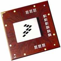
MPC8560CPX667JC Freescale Semiconductor, MPC8560CPX667JC Datasheet - Page 25

MPC8560CPX667JC
Manufacturer Part Number
MPC8560CPX667JC
Description
IC MPU PWRQUICC III 783-FCPBGA
Manufacturer
Freescale Semiconductor
Series
PowerQUICC IIIr
Specifications of MPC8560CPX667JC
Processor Type
MPC85xx PowerQUICC III 32-Bit
Speed
667MHz
Voltage
1.2V
Mounting Type
Surface Mount
Package / Case
783-FCPBGA
Core Size
32 Bit
Program Memory Size
64KB
Cpu Speed
667MHz
Embedded Interface Type
I2C, MII, SPI, TDM, UTOPIA
Digital Ic Case Style
BGA
No. Of Pins
783
Rohs Compliant
No
Family Name
MPC85XX
Device Core
PowerQUICC III
Device Core Size
32b
Frequency (max)
667MHz
Instruction Set Architecture
RISC
Supply Voltage 1 (typ)
1.2V
Operating Supply Voltage (max)
1.26V
Operating Supply Voltage (min)
1.14V
Operating Temp Range
-40C to 105C
Operating Temperature Classification
Industrial
Mounting
Surface Mount
Pin Count
783
Package Type
FCBGA
For Use With
MPC8560ADS-BGA - BOARD APPLICATION DEV 8560
Lead Free Status / RoHS Status
Contains lead / RoHS non-compliant
Features
-
Lead Free Status / Rohs Status
Not Compliant
Available stocks
Company
Part Number
Manufacturer
Quantity
Price
Company:
Part Number:
MPC8560CPX667JC
Manufacturer:
Freescale Semiconductor
Quantity:
10 000
Figure 7
7.2.1.2
Table 22
Freescale Semiconductor
At recommended operating conditions with LV
At recommended operating conditions with LV
GTX_CLK data clock rise and fall time
Notes:
1. The symbols used for timing specifications herein follow the pattern t
2.Signal timings are measured at 0.7 V and 1.9 V voltage levels.
3.Guaranteed by characterization.
4.Guaranteed by design.
RX_CLK clock period
RX_CLK duty cycle
RXD[7:0], RX_DV, RX_ER setup time to RX_CLK
RXD[7:0], RX_DV, RX_ER hold time to RX_CLK
(reference)(state)
symbolizes GMII transmit timing (GT) with respect to the t
to the time date input signals (D) reaching the valid state (V) to state or setup time. Also, t
transmit timing (GT) with respect to the t
input signals (D) going invalid (X) or hold time. Note that, in general, the clock reference symbol representation is
based on three letters representing the clock of a particular functional. For example, the subscript of t
the GMII(G) transmit (TX) clock. For rise and fall times, the latter convention is used with the appropriate letter: R
(rise) or F (fall).
shows the GMII transmit AC timing diagram.
provides the GMII receive AC timing specifications.
GMII Receive AC Timing Specifications
GTX_CLK
Parameter/Condition
TXD[7:0]
Parameter/Condition
TX_EN
TX_ER
for inputs and t
Table 21. GMII Transmit AC Timing Specifications (continued)
MPC8560 Integrated Processor Hardware Specifications, Rev. 4.2
Table 22. GMII Receive AC Timing Specifications
(first two letters of functional block)(reference)(state)(signal)(state)
Figure 7. GMII Transmit AC Timing Diagram
t
GTXH
t
DD
GTKHDV
DD
of 3.3 V ± 5%, or LV
of 3.3 V ± 5%, or LV
t
GTX
GTX
clock reference (K) going to the high state (H) relative to the time date
t
DD
DD
GTXR
t
=2.5V ± 5%.
Symbol
=2.5V ± 5%.
Symbol
GRXH
t
t
GTX
t
GRDVKH
GRDXKH
GTXF
t
, t
GRX
GTXF
/t
clock reference (K) going to the high state (H) relative
t
GRX
GTKHDX
1
1
(first two letters of functional block)(signal)(state)
2,4
t
GTXR
Min
Min
2.0
0.5
40
—
—
Ethernet: Three-Speed, MII Management
for outputs. For example, t
Typ
Typ
8.0
—
—
—
—
GTKHDX
Max
Max
symbolizes GMII
1.0
60
—
—
—
GTX
represents
GTKHDV
Unit
Unit
ns
ns
ns
ns
ns
25


