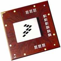
MPC8560CPX667JC Freescale Semiconductor, MPC8560CPX667JC Datasheet - Page 78

MPC8560CPX667JC
Manufacturer Part Number
MPC8560CPX667JC
Description
IC MPU PWRQUICC III 783-FCPBGA
Manufacturer
Freescale Semiconductor
Series
PowerQUICC IIIr
Specifications of MPC8560CPX667JC
Processor Type
MPC85xx PowerQUICC III 32-Bit
Speed
667MHz
Voltage
1.2V
Mounting Type
Surface Mount
Package / Case
783-FCPBGA
Core Size
32 Bit
Program Memory Size
64KB
Cpu Speed
667MHz
Embedded Interface Type
I2C, MII, SPI, TDM, UTOPIA
Digital Ic Case Style
BGA
No. Of Pins
783
Rohs Compliant
No
Family Name
MPC85XX
Device Core
PowerQUICC III
Device Core Size
32b
Frequency (max)
667MHz
Instruction Set Architecture
RISC
Supply Voltage 1 (typ)
1.2V
Operating Supply Voltage (max)
1.26V
Operating Supply Voltage (min)
1.14V
Operating Temp Range
-40C to 105C
Operating Temperature Classification
Industrial
Mounting
Surface Mount
Pin Count
783
Package Type
FCBGA
For Use With
MPC8560ADS-BGA - BOARD APPLICATION DEV 8560
Lead Free Status / RoHS Status
Contains lead / RoHS non-compliant
Features
-
Lead Free Status / Rohs Status
Not Compliant
Available stocks
Company
Part Number
Manufacturer
Quantity
Price
Company:
Part Number:
MPC8560CPX667JC
Manufacturer:
Freescale Semiconductor
Quantity:
10 000
Package and Pin Listings
78
LV
MV
No Connects
OV
RESERVED
SENSEVDD
SENSEVSS
V
PA[0:31]
PB[4:31]
PC[0:31]
DD
DD
DD
REF
Signal
MPC8560 Integrated Processor Hardware Specifications, Rev. 4.2
AA5, AA12, AA16, AA20, AB7, AB9, AB26, AC5, AC11,
AC17, AD4, AE1, AE8, AE10, AE15, AF7, AF12, AG27,
P9, P8, P7, P6, P5, P4, P3, P2, P1, R1, R2, R3, R4, R5,
R8, R9, R10, R11, T9, T6, T5, T4, T1, U1, U2, U3, U4,
U7, U8, U9, U10, V9, V6, V5, V4, V3, V2, V1, W1, W2,
K2, K1, L1, L2, L3, L4, L5, L8, L9, L10, L11, M10, M9,
M1, N1, N4, N5, N6, N7, N8, N9, N10, N11, P11, P10,
T7, U5, U20, U26, V8, W4, W13, W19, W21, Y7, Y23,
M13, M15, M17, N14, N16, P13, P15, P17, R12, R14,
D1, E4, H3, K4, K10, L7, M5, N3, P22, R19, R25, T2,
H1, H2, J1, J2, J3, J4, J5, J6, J7, J8, K8, K7, K6, K3,
Table 54. MPC8560 Pinout Listing (continued)
AH26, AH27, AH28, AG28, AF28, AE28,
AH1, AG1, AH2, B1, B2, A2, A3, AH25
R16, T13, T15, T17, U12, U14
W3, W6, W7, W8, W9, Y9
Package Pin Number
M8, M7, M6, M3, M2
C1, T11, U11, AF1
A4, C5, E7, H10
R6, R7
N27
AH4
K12
L12
CPM
Ethernet, and other
Reference Voltage;
Ethernet I/O (2.5 V,
Reference Voltage
RapidIO, 10/100
Power for Core
Power for Core
Three-Speed
Signal; DDR
PCI/PCI-X,
Pin Type
Standard
(3.3 V)
(1.2 V)
(1.2 V)
3.3 V)
I/0
I/0
I/0
—
—
—
Freescale Semiconductor
Supply
MV
Power
OV
OV
OV
OV
LV
V
V
—
—
—
DD
DD
REF
DD
DD
DD
DD
DD
Notes
16
15
13
13
—
—
—
—
—
—
—


