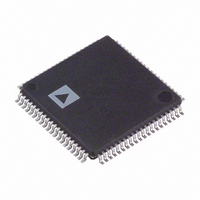
AD9854ASTZ Analog Devices Inc, AD9854ASTZ Datasheet - Page 27

AD9854ASTZ
Manufacturer Part Number
AD9854ASTZ
Description
IC DDS QUADRATURE CMOS 80-LQFP
Manufacturer
Analog Devices Inc
Datasheet
1.AD9854ASTZ.pdf
(52 pages)
Specifications of AD9854ASTZ
Package / Case
80-LQFP
Resolution (bits)
12 b
Master Fclk
300MHz
Tuning Word Width (bits)
48 b
Voltage - Supply
3.14 V ~ 3.47 V
Operating Temperature
-40°C ~ 85°C
Mounting Type
Surface Mount
Supply Voltage Range
3.135V To 3.465V
Operating Temperature Range
-40°C To +85°C
Digital Ic Case Style
LQFP
No. Of Pins
80
Svhc
No SVHC (18-Jun-2010)
Base Number
9854
Ic Function
Direct Digital Synthesizer
Rohs Compliant
Yes
Lead Free Status / RoHS Status
Lead free / RoHS Compliant
For Use With
AD9854/PCBZ - BOARD EVAL FOR AD9854
Lead Free Status / RoHS Status
Lead free / RoHS Compliant, Lead free / RoHS Compliant
Available stocks
Company
Part Number
Manufacturer
Quantity
Price
Company:
Part Number:
AD9854ASTZ
Manufacturer:
Renesas
Quantity:
103
Company:
Part Number:
AD9854ASTZ
Manufacturer:
ADI
Quantity:
271
Company:
Part Number:
AD9854ASTZ
Manufacturer:
Analog Devices Inc
Quantity:
10 000
Part Number:
AD9854ASTZ
Manufacturer:
ADI/亚德诺
Quantity:
20 000
The 32-bit automatic I/O update counter can be used to
construct complex chirp or ramped FSK sequences. Because
this internal counter is synchronized with the AD9854 system
clock, precisely timed program changes are possible. For such
changes, the user need only reprogram the desired registers
before the automatic I/O update clock is generated.
In chirp mode, the destination frequency is not directly specified.
If the user fails to control the chirp, the DDS automatically confines
itself to the frequency range between dc and Nyquist. Unless
terminated by the user, the chirp continues until power is removed.
When the chirp destination frequency is reached, the user can
choose any of the following actions:
PHASE ADJUST 1
PHASE ADJUST 2
RAMP RATE
I/O UD CLK
BPSK DATA
I/O UD CLK
MODE
HOLD
DFW
TW1
MODE
FTW1
000 (DEFAULT)
F1
000 (DEFAULT)
0
360
0
0
0
Figure 47. Example of Hold Function
Figure 48. BPSK Mode
Rev. E | Page 27 of 52
DELTA FREQUENCY WORD
RAMP RATE
011 (CHIRP)
•
•
•
•
100 (BPSK)
F1
270°
Stop at the destination frequency by using the HOLD pin
or by loading all 0s into the delta frequency word registers
of the frequency accumulator (ACC1).
Use the HOLD pin function to stop the chirp, and then ramp
down the output amplitude by using the digital multiplier
stages and the output shaped keying pin (Pin 30), or by using
the program register control (Address 21 to Address 24 hex).
Abruptly end the transmission with the CLR ACC2 bit.
Continue chirp by reversing direction and returning to
the previous or another destination frequency in a linear or
user-directed manner. If this involves reducing the
frequency, a negative 48-bit delta frequency word (the
MSB is set to 1) must be loaded into Register 10 hex to
Register 15 hex. Any decreasing frequency step of the delta
frequency word requires the MSB to be set to logic high.
90°
F1
AD9854


