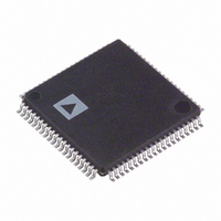
AD9854ASTZ Analog Devices Inc, AD9854ASTZ Datasheet - Page 34

AD9854ASTZ
Manufacturer Part Number
AD9854ASTZ
Description
IC DDS QUADRATURE CMOS 80-LQFP
Manufacturer
Analog Devices Inc
Datasheet
1.AD9854ASTZ.pdf
(52 pages)
Specifications of AD9854ASTZ
Package / Case
80-LQFP
Resolution (bits)
12 b
Master Fclk
300MHz
Tuning Word Width (bits)
48 b
Voltage - Supply
3.14 V ~ 3.47 V
Operating Temperature
-40°C ~ 85°C
Mounting Type
Surface Mount
Supply Voltage Range
3.135V To 3.465V
Operating Temperature Range
-40°C To +85°C
Digital Ic Case Style
LQFP
No. Of Pins
80
Svhc
No SVHC (18-Jun-2010)
Base Number
9854
Ic Function
Direct Digital Synthesizer
Rohs Compliant
Yes
Lead Free Status / RoHS Status
Lead free / RoHS Compliant
For Use With
AD9854/PCBZ - BOARD EVAL FOR AD9854
Lead Free Status / RoHS Status
Lead free / RoHS Compliant, Lead free / RoHS Compliant
Available stocks
Company
Part Number
Manufacturer
Quantity
Price
Company:
Part Number:
AD9854ASTZ
Manufacturer:
Renesas
Quantity:
103
Company:
Part Number:
AD9854ASTZ
Manufacturer:
ADI
Quantity:
271
Company:
Part Number:
AD9854ASTZ
Manufacturer:
Analog Devices Inc
Quantity:
10 000
Part Number:
AD9854ASTZ
Manufacturer:
ADI/亚德诺
Quantity:
20 000
AD9854
PARALLEL I/O OPERATION
With the S/P SELECT pin tied high, the parallel I/O mode is active.
The I/O port is compatible with industry-standard DSPs and
microcontrollers. Six address bits, eight bidirectional data bits,
and separate write/read control inputs comprise the I/O port pins.
Parallel I/O operation allows write access to each byte of any
register in a single I/O operation of up to one per 10.5 ns.
Readback capability for each register is included to ease designing
with the AD9854. (Reads are not guaranteed at 100 MHz because
they are intended for software debugging only.)
Parallel I/O operation timing diagrams are shown in Figure 52
and Figure 53.
SERIAL PORT I/O OPERATION
With the S/P SELECT pin tied low, the serial I/O mode is active.
The serial port is a flexible, synchronous, serial communication
port, allowing easy interface to many industry-standard micro-
controllers and microprocessors. The serial I/O is compatible
with most synchronous transfer formats, including both the
Motorola® 6905/11 SPI and Intel® 8051 SSR protocols. The
Table 9. Serial I/O Pin Requirements
Pin Number
1 to 8
14 to 16
17
18
19
20
21
22
Mnemonic
D [7:0]
A [5:3]
A2/IO RESET
A1/SDO
A0/SDIO
I/O UD CLK
WR/SCLK
RD/CS
Serial I/O Description
The parallel data pins are not active; tie to VDD or GND.
The A5, A4, and A3 parallel address pins are not active; tie these pins to VDD or GND.
IO RESET.
SDO.
SDIO.
Update Clock. Same functionality for serial mode as parallel mode.
SCLK.
CS—Chip Select.
Rev. E | Page 34 of 52
interface allows read/write access to all 12 registers that configure
the AD9854 and can be configured as a single-pin I/O (SDIO) or
two unidirectional pins for input and output (SDIO/SDO). Data
transfers are supported in MSB-or the LSB-first format for up
to 10 MHz.
When configured for serial I/O operation, most AD9854 parallel
port pins are inactive; only some pins are used for the serial I/O
operation. Table 9 describes pin requirements for serial I/O
operation.
Note that when operating the device in serial I/O mode, it
is best to use the external I/O update clock mode to avoid an
update occurring during a serial communication cycle. Such an
occurrence may cause incorrect programming due to a partial
data transfer. To exit the default internal update mode, program
the device for external update operation at power-up before
starting the REFCLK signal but after a master reset. Starting the
REFCLK causes this information to transfer to the register bank,
forcing the device to switch to external update mode.


