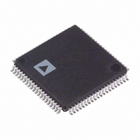
AD9854ASTZ Analog Devices Inc, AD9854ASTZ Datasheet - Page 9

AD9854ASTZ
Manufacturer Part Number
AD9854ASTZ
Description
IC DDS QUADRATURE CMOS 80-LQFP
Manufacturer
Analog Devices Inc
Datasheet
1.AD9854ASTZ.pdf
(52 pages)
Specifications of AD9854ASTZ
Package / Case
80-LQFP
Resolution (bits)
12 b
Master Fclk
300MHz
Tuning Word Width (bits)
48 b
Voltage - Supply
3.14 V ~ 3.47 V
Operating Temperature
-40°C ~ 85°C
Mounting Type
Surface Mount
Supply Voltage Range
3.135V To 3.465V
Operating Temperature Range
-40°C To +85°C
Digital Ic Case Style
LQFP
No. Of Pins
80
Svhc
No SVHC (18-Jun-2010)
Base Number
9854
Ic Function
Direct Digital Synthesizer
Rohs Compliant
Yes
Lead Free Status / RoHS Status
Lead free / RoHS Compliant
For Use With
AD9854/PCBZ - BOARD EVAL FOR AD9854
Lead Free Status / RoHS Status
Lead free / RoHS Compliant, Lead free / RoHS Compliant
Available stocks
Company
Part Number
Manufacturer
Quantity
Price
Company:
Part Number:
AD9854ASTZ
Manufacturer:
Renesas
Quantity:
103
Company:
Part Number:
AD9854ASTZ
Manufacturer:
ADI
Quantity:
271
Company:
Part Number:
AD9854ASTZ
Manufacturer:
Analog Devices Inc
Quantity:
10 000
Part Number:
AD9854ASTZ
Manufacturer:
ADI/亚德诺
Quantity:
20 000
PIN CONFIGURATION AND FUNCTION DESCRIPTIONS
Table 4. Pin Function Descriptions
Pin No.
1 to 8
9, 10, 23, 24, 25,
73, 74, 79, 80
11, 12, 26, 27, 28,
72, 75 to 78
13, 35, 57, 58, 63
14 to 16
17
18
19
Mnemonic
D7 to D0
DVDD
DGND
NC
A5 to A3
A2/IO RESET
A1/SDO
A0/SDIO
NC = NO CONNECT
A2/IO RESET
I/O UD CLK
A0/SDIO
A1/SDO
DGND
DGND
DVDD
DVDD
NC
D7
D6
D5
D4
D3
D2
D1
D0
A5
A4
A3
Description
8-Bit Bidirectional Parallel Programming Data Inputs. Used only in parallel programming mode.
Connections for the Digital Circuitry Supply Voltage. Nominally 3.3 V more positive than AGND
and DGND.
Connections for the Digital Circuitry Ground Return. Same potential as AGND.
No Internal Connection.
Parallel Address Inputs for Program Registers (Part of 6-Bit Parallel Address Inputs for Program
Register, A5:A0). Used only in parallel programming mode.
Parallel Address Input for Program Registers (Part of 6-Bit Parallel Address Inputs for Program
Register, A5:A0)/IO Reset. A2 is used only in parallel programming mode. IO RESET is used when
the serial programming mode is selected, allowing an IO RESET of the serial communication bus
that is unresponsive due to improper programming protocol. Resetting the serial bus in this
manner does not affect previous programming, nor does it invoke the default programming
values listed in Table 8. Active high.
Parallel Address Input for Program Registers (Part of 6-Bit Parallel Address Inputs for Program
Register, A5:A0)/Unidirectional Serial Data Output. A1 is used only in parallel programming
mode. SDO is used in 3-wire serial communication mode when the serial programming mode is
selected.
Parallel Address Input for Program Registers (Part of 6-Bit Parallel Address Inputs for Program
Register, A5:A0)/Bidirectional Serial Data I/O. A0 is used only in parallel programming mode. SDIO
is used in 2-wire serial communication mode.
10
11
12
13
14
15
16
17
18
19
20
1
2
3
4
5
6
7
8
9
80 79 78 77 76
21 22 23 24 25 26 27 28 29 30 31 32 33
PIN 1
INDICATOR
Figure 2. Pin Configuration
75 74 73 72
Rev. E | Page 9 of 52
(Not to Scale)
AD9854
TOP VIEW
71 70 69 68
67 66 65
34 35 36 37 38 39 40
64 63 62 61
60
59
58
57
56
55
54
53
52
51
50
49
48
47
46
45
44
43
42
41
AVDD
AGND
NC
NC
DAC R
DACBP
AVDD
AGND
IOUT2
IOUT2
AVDD
IOUT1
IOUT1
AGND
AGND
AGND
AVDD
VINN
VINP
AGND
SET
AD9854


