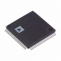
AD9854ASTZ Analog Devices Inc, AD9854ASTZ Datasheet - Page 39

AD9854ASTZ
Manufacturer Part Number
AD9854ASTZ
Description
IC DDS QUADRATURE CMOS 80-LQFP
Manufacturer
Analog Devices Inc
Datasheet
1.AD9854ASTZ.pdf
(52 pages)
Specifications of AD9854ASTZ
Package / Case
80-LQFP
Resolution (bits)
12 b
Master Fclk
300MHz
Tuning Word Width (bits)
48 b
Voltage - Supply
3.14 V ~ 3.47 V
Operating Temperature
-40°C ~ 85°C
Mounting Type
Surface Mount
Supply Voltage Range
3.135V To 3.465V
Operating Temperature Range
-40°C To +85°C
Digital Ic Case Style
LQFP
No. Of Pins
80
Svhc
No SVHC (18-Jun-2010)
Base Number
9854
Ic Function
Direct Digital Synthesizer
Rohs Compliant
Yes
Lead Free Status / RoHS Status
Lead free / RoHS Compliant
For Use With
AD9854/PCBZ - BOARD EVAL FOR AD9854
Lead Free Status / RoHS Status
Lead free / RoHS Compliant, Lead free / RoHS Compliant
Available stocks
Company
Part Number
Manufacturer
Quantity
Price
Company:
Part Number:
AD9854ASTZ
Manufacturer:
Renesas
Quantity:
103
Company:
Part Number:
AD9854ASTZ
Manufacturer:
ADI
Quantity:
271
Company:
Part Number:
AD9854ASTZ
Manufacturer:
Analog Devices Inc
Quantity:
10 000
Part Number:
AD9854ASTZ
Manufacturer:
ADI/亚德诺
Quantity:
20 000
CR [8] is the internal update active bit. When this bit is set to
Logic 1, the I/O UD CLK pin is an output and the AD9854
generates the I/O UD CLK signal. When this bit is set to Logic 0,
external I/O UD CLK functionality is performed and the I/O
UD CLK pin is configured as an input.
CR [7] is reserved. Write to 0.
CR [6] is the inverse sinc filter bypass bit. When this bit is set,
the data from the DDS block goes directly to the output shaped
keying logic, and the clock to the inverse sinc filter is stopped.
Default is clear with the filter enabled.
CR [5] is the shaped keying enable bit. When this bit is set, the
output ramping function is enabled and is performed in
accordance with the CR [4] bit requirements.
SCLK
SDIO
SCLK
CS
SCLK
SCLK
SDIO
SDIO
SDIO
SDO
CS
CS
CS
I
7
I
7
I
7
I
7
I
6
I
6
I
6
I
6
INSTRUCTION CYCLE
I
5
INSTRUCTION CYCLE
INSTRUCTION CYCLE
INSTRUCTION CYCLE
I
I
5
I
5
5
I
4
I
I
4
I
4
4
Figure 61. 2-Wire Serial Port Read Timing Clock Stall High
Figure 59. 3-Wire Serial Port Read Timing Clock Stall Low
I
3
Figure 60. Serial Port Write Timing Clock Stall High
Figure 58. Serial Port Write Timing Clock Stall Low
I
I
I
3
3
3
I
2
I
I
I
2
2
2
I
1
I
I
1
I
1
Rev. E | Page 39 of 52
1
I
0
I
I
0
0
I
0
D
O7
CR [4] is the internal/external output shaped keying control bit.
When this bit is set to Logic 1, the output shaped keying factor is
internally generated and applied to both the I and Q paths.
When this bit is cleared (default), the output shaped keying
function is externally controlled by the user, and the ouput
shaped keying factor is the value of the I and Q output shaped
keying factor register. The two registers that are the output
shaped keying factors also default low such that the output is off
at power-up until the device is programmed by the user.
CR [3:2] are reserved. Write to 0.
CR [1] is the serial port MSB-/LSB-first bit. Default is low,
MSB first.
CR [0] is the serial port SDO active bit. Default is low, inactive.
D
D
7
7
D
O7
D
O6
D
6
D
D
O6
6
D
O5
D
DATA TRANSFER CYCLE
5
D
DATA TRANSFER CYCLE
DATA TRANSFER CYCLE
DATA TRANSFER CYCLE
O5
D
D
5
O4
D
4
DON'T CARE
D
O4
D
D
O3
4
D
3
D
O3
D
O2
D
D
D
3
2
O2
D
O1
D
D
D
1
O1
2
D
D
D
O0
0
O0
D
1
D
0
AD9854


