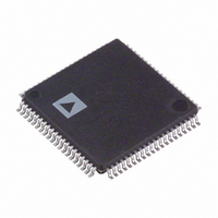
AD9854ASTZ Analog Devices Inc, AD9854ASTZ Datasheet - Page 38

AD9854ASTZ
Manufacturer Part Number
AD9854ASTZ
Description
IC DDS QUADRATURE CMOS 80-LQFP
Manufacturer
Analog Devices Inc
Datasheet
1.AD9854ASTZ.pdf
(52 pages)
Specifications of AD9854ASTZ
Package / Case
80-LQFP
Resolution (bits)
12 b
Master Fclk
300MHz
Tuning Word Width (bits)
48 b
Voltage - Supply
3.14 V ~ 3.47 V
Operating Temperature
-40°C ~ 85°C
Mounting Type
Surface Mount
Supply Voltage Range
3.135V To 3.465V
Operating Temperature Range
-40°C To +85°C
Digital Ic Case Style
LQFP
No. Of Pins
80
Svhc
No SVHC (18-Jun-2010)
Base Number
9854
Ic Function
Direct Digital Synthesizer
Rohs Compliant
Yes
Lead Free Status / RoHS Status
Lead free / RoHS Compliant
For Use With
AD9854/PCBZ - BOARD EVAL FOR AD9854
Lead Free Status / RoHS Status
Lead free / RoHS Compliant, Lead free / RoHS Compliant
Available stocks
Company
Part Number
Manufacturer
Quantity
Price
Company:
Part Number:
AD9854ASTZ
Manufacturer:
Renesas
Quantity:
103
Company:
Part Number:
AD9854ASTZ
Manufacturer:
ADI
Quantity:
271
Company:
Part Number:
AD9854ASTZ
Manufacturer:
Analog Devices Inc
Quantity:
10 000
Part Number:
AD9854ASTZ
Manufacturer:
ADI/亚德诺
Quantity:
20 000
AD9854
MSB/LSB TRANSFERS
The AD9854 serial port can support MSB- and LSB-first data
formats. This functionality is controlled by Bit 1 of Serial
Register Bank 20 hex. When this bit is set active high, the
AD9854 serial port is in LSB-first format. This bit defaults low,
to the MSB-first format. The instruction byte must be written in
the format indicated by Bit 1 of Serial Register Bank 20 hex.
Therefore, if the AD9854 is in LSB-first mode, the instruction
byte must be written from least significant bit to most
significant bit.
CONTROL REGISTER DESCRIPTION
The control register is located in the shaded portion of Table 8
at Address 1D to Address 20 hex. It is composed of 32 bits.
Bit 31 is located at the top left position, and Bit 0 is located in
the lower right position of the shaded portion. In the text that
follows, the register descriptions have been subdivided to make it
easier to locate the text associated with specific control categories.
CR [31:29] are open.
CR [28] is the comparator power-down bit. When this bit is set
(Logic 1), its signal indicates to the comparator that a power-
down mode is active. This bit is an output of the digital section
and is an input to the analog section.
CR [27] must always be written to Logic 0. Writing this bit to
Logic 1 causes the AD9854 to stop functioning until a master
reset is applied.
CR [26] is the Q DAC power-down bit. When this bit is set
(Logic 1), it indicates to the Q DAC that a power-down mode
is active.
CR [25] is the full DAC power-down bit. When this bit is set
(Logic 1), it indicates to both the I and Q DACs, as well as the
reference, that a power-down mode is active.
CR [24] is the digital power-down bit. When this bit is set
(Logic 1), its signal indicates to the digital section that a power-
down mode is active. Within the digital section, the clocks are
forced to dc, effectively powering down the digital section. In
this state, the PLL still accepts the REFCLK signal and
continues to output the higher frequency.
CR [23] is reserved. Write to 0.
Rev. E | Page 38 of 52
CR [22] is the PLL range bit, which controls the VCO gain. The
power-up state of the PLL range bit is Logic 1; a higher gain is
required for frequencies greater than 200 MHz.
CR [21] is the bypass PLL bit, active high. When this bit is
active, the PLL is powered down and the REFCLK input is used
to drive the system clock signal. The power-up state of the
bypass PLL bit is Logic 1 with PLL bypassed.
CR [20:16] bits are the PLL multiplier factor. These bits are the
REFCLK multiplication factor unless the bypass PLL bit is set.
The PLL multiplier valid range is from 4 to 20, inclusive.
CR [15] is the Clear Accumulator 1 bit. This bit has a one-shot
type of function. When this bit is written active (Logic 1), a
Clear Accumulator 1 signal is sent to the DDS logic, resetting
the accumulator value to 0. The bit is then automatically reset,
but the buffer memory is not reset. This bit allows the user to
easily create a sawtooth frequency sweep pattern with minimal
intervention. This bit is intended for chirp mode only, but its
function is still retained in other modes.
CR [14] is the clear accumulator bit. When this bit is active high,
it holds both the Accumulator 1 and Accumulator 2 values at 0
for as long as the bit is active. This allows the DDS phase to be
initialized via the I/O port.
CR [13] is the triangle bit. When this bit is set, the AD9854
automatically performs a continuous frequency sweep from F1
to F2 frequencies and back. This results in a triangular
frequency sweep. When this bit is set, the operating mode must
be set to ramped FSK.
CR [12] is the source Q DAC bit. When this bit is set high, the
Q path DAC accepts data from the Q DAC register.
CR [11:9] are the three bits that describe the five operating
modes of the AD9854:
0x0 = single-tone mode
0x1 = FSK mode
0x2 = ramped FSK mode
0x3 = chirp mode
0x4 = BPSK mode


