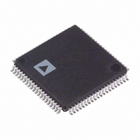
AD9854ASTZ Analog Devices Inc, AD9854ASTZ Datasheet - Page 28

AD9854ASTZ
Manufacturer Part Number
AD9854ASTZ
Description
IC DDS QUADRATURE CMOS 80-LQFP
Manufacturer
Analog Devices Inc
Datasheet
1.AD9854ASTZ.pdf
(52 pages)
Specifications of AD9854ASTZ
Package / Case
80-LQFP
Resolution (bits)
12 b
Master Fclk
300MHz
Tuning Word Width (bits)
48 b
Voltage - Supply
3.14 V ~ 3.47 V
Operating Temperature
-40°C ~ 85°C
Mounting Type
Surface Mount
Supply Voltage Range
3.135V To 3.465V
Operating Temperature Range
-40°C To +85°C
Digital Ic Case Style
LQFP
No. Of Pins
80
Svhc
No SVHC (18-Jun-2010)
Base Number
9854
Ic Function
Direct Digital Synthesizer
Rohs Compliant
Yes
Lead Free Status / RoHS Status
Lead free / RoHS Compliant
For Use With
AD9854/PCBZ - BOARD EVAL FOR AD9854
Lead Free Status / RoHS Status
Lead free / RoHS Compliant, Lead free / RoHS Compliant
Available stocks
Company
Part Number
Manufacturer
Quantity
Price
Company:
Part Number:
AD9854ASTZ
Manufacturer:
Renesas
Quantity:
103
Company:
Part Number:
AD9854ASTZ
Manufacturer:
ADI
Quantity:
271
Company:
Part Number:
AD9854ASTZ
Manufacturer:
Analog Devices Inc
Quantity:
10 000
Part Number:
AD9854ASTZ
Manufacturer:
ADI/亚德诺
Quantity:
20 000
AD9854
•
BPSK (Mode 100)
Binary, biphase, or bipolar phase shift keying is a means to
rapidly select between two preprogrammed 14-bit output phase
offsets that equally affect both the I and Q outputs of the
AD9854. The logic state of Pin 29, the BPSK pin, controls the
Continue chirp by immediately returning to the beginning
frequency (F1) in a sawtooth fashion, and then repeating the
previous chirp process using the CLR ACC1 control bit.
An automatic, repeating chirp can be set up by using the
32-bit update clock to issue the CLR ACC1 command at
precise time intervals. Adjusting the timing intervals or
changing the delta frequency word changes the chirp
range. It is incumbent upon the user to balance the chirp
duration and frequency resolution to achieve the proper
frequency range.
Rev. E | Page 28 of 52
selection of Phase Adjust Register 1 or Phase Adjust Register 2.
When low, Pin 29 selects Phase Adjust Register 1; when hig
selects Phase Adjust Register 2. Figure 48 illustrate
changes made to four cycles of an out
Basic BPSK Programming Steps
1.
2.
3.
4.
Note that for higher-order PSK modulation, the user can sele
the single-tone mode and program Phase Adjust Register
using the serial or high speed parallel programming bus.
Program a carrier frequency into Frequency Tuning Word 1.
Program the appropriate 14-bit phase words int
Adjust Register 1 and Phase Adjust Regi
Attach the BPSK data source to Pin 29.
Activate the I/O update clock when ready.
put carrier.
ster 2.
s phase
o Phase
1
h, it
ct


