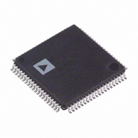
AD9854ASTZ Analog Devices Inc, AD9854ASTZ Datasheet - Page 8

AD9854ASTZ
Manufacturer Part Number
AD9854ASTZ
Description
IC DDS QUADRATURE CMOS 80-LQFP
Manufacturer
Analog Devices Inc
Datasheet
1.AD9854ASTZ.pdf
(52 pages)
Specifications of AD9854ASTZ
Package / Case
80-LQFP
Resolution (bits)
12 b
Master Fclk
300MHz
Tuning Word Width (bits)
48 b
Voltage - Supply
3.14 V ~ 3.47 V
Operating Temperature
-40°C ~ 85°C
Mounting Type
Surface Mount
Supply Voltage Range
3.135V To 3.465V
Operating Temperature Range
-40°C To +85°C
Digital Ic Case Style
LQFP
No. Of Pins
80
Svhc
No SVHC (18-Jun-2010)
Base Number
9854
Ic Function
Direct Digital Synthesizer
Rohs Compliant
Yes
Lead Free Status / RoHS Status
Lead free / RoHS Compliant
For Use With
AD9854/PCBZ - BOARD EVAL FOR AD9854
Lead Free Status / RoHS Status
Lead free / RoHS Compliant, Lead free / RoHS Compliant
Available stocks
Company
Part Number
Manufacturer
Quantity
Price
Company:
Part Number:
AD9854ASTZ
Manufacturer:
Renesas
Quantity:
103
Company:
Part Number:
AD9854ASTZ
Manufacturer:
ADI
Quantity:
271
Company:
Part Number:
AD9854ASTZ
Manufacturer:
Analog Devices Inc
Quantity:
10 000
Part Number:
AD9854ASTZ
Manufacturer:
ADI/亚德诺
Quantity:
20 000
AD9854
ABSOLUTE MAXIMUM RATINGS
Table 2.
Parameter
Maximum Junction Temperature
V
Digital Inputs
Digital Output Current
Storage Temperature Range
Operating Temperature Range
Lead Temperature (Soldering, 10 sec)
Maximum Clock Frequency (ASVZ)
Maximum Clock Frequency (ASTZ)
Stresses above those listed under Absolute Maximum Ratings
may cause permanent damage to the device. This is a stress
rating only; functional operation of the device at these or any
other conditions above those indicated in the operational
section of this specification is not implied. Exposure to absolute
maximum rating conditions for extended periods may affect
device reliability.
THERMAL RESISTANCE
The heat sink of the AD9854ASVZ 80-lead TQFP package must
be soldered to the PCB.
Table 3.
Thermal Characteristic
θ
θ
θ
Ψ
θ
1
2
3
4
5
6
7
Per JEDEC JESD51-2 (heat sink soldered to PCB).
2S2P JEDEC test board.
Values of θ
considerations.
Per JEDEC JESD51-6 (heat sink soldered to PCB).
Airflow increases heat dissipation, effectively reducing θ
more metal that is directly in contact with the package leads from metal
traces through holes, ground, and power planes, the more θ
Per MIL-Std 883, Method 1012.1.
Values of θ
considerations when an external heat sink is required.
JA
JMA
JMA
JC
S
JT
6, 7
1, 2
(0 m/sec airflow)
(1.0 m/sec airflow)
(2.5 m/sec airflow)
JA
JC
are provided for package comparison and PCB design
are provided for package comparison and PCB design
1, 2, 3
2, 3, 4, 5
2, 3, 4, 5
TQFP
16.2°C/W
13.7°C/W
12.8°C/W
0.3°C/W
2.0°C/W
Rating
150°C
4 V
−0.7 V to +V
5 mA
−65°C to +150°C
−40°C to +85°C
300°C
300 MHz
200 MHz
JA
. Furthermore, the
LQFP
38°C/W
JA
is reduced.
S
Rev. E | Page 8 of 52
To determine the junction temperature on the application PCB
use the following equation:
where:
T
T
measured by the user at the top center of the package.
Ψ
PD is the power dissipation (PD); see the Power Dissipation and
Thermal Considerations section for the method to calculate PD.
EXPLANATION OF TEST LEVELS
Table 3.
Test Level
I
III
IV
V
VI
ESD CAUTION
J
case
JT
is the junction temperature expressed in degrees Celsius.
= 0.3°C/W.
is the case temperature expressed in degrees Celsius, as
T
J
= T
case
+ (
Description
100% production tested.
Sample tested only.
Parameter is guaranteed by design and
characterization testing.
Parameter is a typical value only.
Devices are 100% production tested at 25°C and
guaranteed by design and characterization testing
for industrial operating temperature range.
Ψ
JT
× PD)


