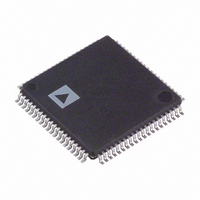
AD9854ASTZ Analog Devices Inc, AD9854ASTZ Datasheet - Page 29

AD9854ASTZ
Manufacturer Part Number
AD9854ASTZ
Description
IC DDS QUADRATURE CMOS 80-LQFP
Manufacturer
Analog Devices Inc
Datasheet
1.AD9854ASTZ.pdf
(52 pages)
Specifications of AD9854ASTZ
Package / Case
80-LQFP
Resolution (bits)
12 b
Master Fclk
300MHz
Tuning Word Width (bits)
48 b
Voltage - Supply
3.14 V ~ 3.47 V
Operating Temperature
-40°C ~ 85°C
Mounting Type
Surface Mount
Supply Voltage Range
3.135V To 3.465V
Operating Temperature Range
-40°C To +85°C
Digital Ic Case Style
LQFP
No. Of Pins
80
Svhc
No SVHC (18-Jun-2010)
Base Number
9854
Ic Function
Direct Digital Synthesizer
Rohs Compliant
Yes
Lead Free Status / RoHS Status
Lead free / RoHS Compliant
For Use With
AD9854/PCBZ - BOARD EVAL FOR AD9854
Lead Free Status / RoHS Status
Lead free / RoHS Compliant, Lead free / RoHS Compliant
Available stocks
Company
Part Number
Manufacturer
Quantity
Price
Company:
Part Number:
AD9854ASTZ
Manufacturer:
Renesas
Quantity:
103
Company:
Part Number:
AD9854ASTZ
Manufacturer:
ADI
Quantity:
271
Company:
Part Number:
AD9854ASTZ
Manufacturer:
Analog Devices Inc
Quantity:
10 000
Part Number:
AD9854ASTZ
Manufacturer:
ADI/亚德诺
Quantity:
20 000
USING THE AD9854
INTERNAL AND EXTERNAL UPDATE CLOCK
This update clock function is comprised of a bidirectional
I/O pin (Pin 20) and a programmable 32-bit down-counter. To
program changes that are to be transferred from the I/O buffer
registers to the active core of the DDS, a clock signal (low-to-
high edge) must be externally supplied to Pin 20 or internally
generated by the 32-bit update clock.
When the user provides an external update clock, it is internally
synchronized with the system clock to prevent a partial transfer
of program register information due to a violation of data setup
or hold time. This mode allows the user to completely control when
updated program information becomes effective. The default
mode for the update clock is internal (the internal update clock
control register bit is logic high). To switch to external update
clock mode, the internal update clock control register bit must
be set to logic low. The internal update mode generates automatic,
periodic update pulses at intervals set by the user.
An internally generated update clock can be established by
programming the 32-bit update clock registers (Address 16 hex
to Address 19 hex) and setting the internal update clock control
register bit (Address 1F hex) to logic high. The update clock
down-counter function operates at half the rate of the system
clock (150 MHz maximum) and counts down from a 32-bit
binary value (programmed by the user). When the count
reaches 0, an automatic I/O update of the DDS output or
functions is generated. The update clock is internally and
externally routed to Pin 20 to allow users to synchronize the
programming of update information with the update clock rate.
The time between update pulses is given as
where N is the 32-bit value programmed by the user, and the
allowable range of N is from 1 to (2
The internally generated update pulse that is output from Pin 20
has a fixed high time of eight system clock cycles.
Programming the update clock register to a value less than five
causes the I/O UD CLK pin to remain high. Although the update
clock can function in this state, it cannot be used to indicate when
data is transferring. This is an effect of the minimum high pulse
time when I/O UD CLK functions as an output.
(N + 1)(System Clock Period × 2)
32
− 1).
Rev. E | Page 29 of 52
ON/OFF OUTPUT SHAPED KEYING (OSK)
The on/off OSK feature allows the user to control the amplitude vs.
time slope of the I and Q DAC output signals. This function is
used in burst transmissions of digital data to reduce the adverse
spectral impact of short, abrupt bursts of data. Users must first
enable the digital multipliers by setting the OSK EN bit (Control
Register Address 20 hex) to logic high in the control register.
Otherwise, if the OSK EN bit is set low, the digital multipliers
responsible for amplitude control are bypassed and the I and
Q DAC outputs are set to full-scale amplitude.
In addition to setting the OSK EN bit, a second control bit, OSK
INT (also at Address 20 hex), must be set to logic high. Logic high
selects the linear internal control of the output ramp-up or ramp-
down function. A logic low in the OSK INT bit switches control
of the digital multipliers to user-programmable 12-bit registers,
allowing users to dynamically shape the amplitude transition in
practically any fashion. These 12-bit registers, labeled Output
Shape Key I and Output Shape Key Q, are located at Address 21 hex
through Address 24 hex, as listed in Table 8. The maximum output
amplitude is a function of the R
when OSK INT is enabled.
The transition time from zero scale to full scale must also be
programmed. The transition time is a function of two fixed
elements and one variable. The variable element is the program-
mable 8-bit ramp rate counter. This is a down-counter that is
clocked at the system clock rate (300 MHz maximum) and that
generates one pulse whenever the counter reaches 0. This pulse
is routed to a 12-bit counter that increments with each pulse
received. The outputs of the 12-bit counter are connected to the
12-bit digital multiplier. When the digital multiplier has a value
of all 0s at its inputs, the input signal is multiplied by 0, producing
zero scale. When the multiplier has a value of all 1s, the input
signal is multiplied by a value of 4095 or 4096, producing nearly
full scale. There are 4094 remaining fractional multiplier values that
produce output amplitudes scaled according to their binary values.
SCALE
SCALE
ZERO
ZERO
Figure 49. On/Off Output Shaped Keying
SHAPED ON/OFF KEYING
ABRUPT ON/OFF KEYING
SET
resistor and is not programmable
AD9854
FULL
SCALE
FULL
SCALE


