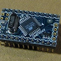
A000003 Arduino, A000003 Datasheet - Page 162
A000003
Manufacturer Part Number
A000003
Description
MCU, MPU & DSP Development Tools MINI
Manufacturer
Arduino
Series
-r
Type
MCUr
Specifications of A000003
Processor To Be Evaluated
Atmega328
Processor Series
ATmega
Data Bus Width
8 bit
Interface Type
USB, RS-232
Operating Supply Voltage
7 V to 9 V
Contents
Board
Lead Free Status / Rohs Status
Lead free / RoHS Compliant
For Use With/related Products
ATmega168


162
ATmega48/88/168
Flag, SPIF is set. If the SPI Interrupt Enable bit, SPIE, in the SPCR Register is set, an interrupt
is requested. The Slave may continue to place new data to be sent into SPDR before reading
the incoming data. The last incoming byte will be kept in the Buffer Register for later use.
Figure 18-2. SPI Master-slave Interconnection
The system is single buffered in the transmit direction and double buffered in the receive direc-
tion. This means that bytes to be transmitted cannot be written to the SPI Data Register before
the entire shift cycle is completed. When receiving data, however, a received character must be
read from the SPI Data Register before the next character has been completely shifted in. Oth-
erwise, the first byte is lost.
In SPI Slave mode, the control logic will sample the incoming signal of the SCK pin. To ensure
correct sampling of the clock signal, the minimum low and high periods should be:
Low periods: Longer than 2 CPU clock cycles.
High periods: Longer than 2 CPU clock cycles.
When the SPI is enabled, the data direction of the MOSI, MISO, SCK, and SS pins is overridden
according to
“Alternate Port Functions” on page
Table 18-1.
Note:
The following code examples show how to initialize the SPI as a Master and how to perform a
simple transmission. DDR_SPI in the examples must be replaced by the actual Data Direction
Register controlling the SPI pins. DD_MOSI, DD_MISO and DD_SCK must be replaced by the
actual data direction bits for these pins. For example if MOSI is placed on pin PB3, replace
DD_MOSI with DDB3 and DDR_SPI with DDRB.
MOSI
MISO
SCK
Pin
SS
See
direction of the user defined SPI pins.
“Alternate Functions of Port B” on page 77
Table 18-1 on page
SPI Pin Overrides
Direction, Master SPI
User Defined
Input
User Defined
User Defined
(Note:)
162. For more details on automatic port overrides, refer to
75.
for a detailed description of how to define the
Direction, Slave SPI
Input
User Defined
Input
Input
SHIFT
ENABLE
2545S–AVR–07/10
Related parts for A000003
Image
Part Number
Description
Manufacturer
Datasheet
Request
R

Part Number:
Description:
Daughter Cards & OEM Boards ARDUINO UNO PROTO PCB REV 3
Manufacturer:
Arduino
Part Number:
Description:
Daughter Cards & OEM Boards ARDUINO SHIELD PROTO KIT REV 3
Manufacturer:
Arduino
Part Number:
Description:
Daughter Cards & OEM Boards ARDUINO MEGA PROTO KIT REV 3
Manufacturer:
Arduino
Part Number:
Description:
Daughter Cards & OEM Boards ARDUINO MEGA PROTO PCB REV 3
Manufacturer:
Arduino
Part Number:
Description:
Development Boards & Kits - AVR ARDUINO STARTER KIT W/ UNO REV3
Manufacturer:
Arduino
Part Number:
Description:
RF Development Tools ARDUINO SHIELD WIRELESS PROTO
Manufacturer:
Arduino
Datasheet:
Part Number:
Description:
RF Development Tools ARDUINO SHIELD WIRELESS WITH SD
Manufacturer:
Arduino
Datasheet:

Part Number:
Description:
Development Software Getting started w/Arduino
Manufacturer:
Arduino

Part Number:
Description:
Ethernet Modules & Development Tools Ethernet Shield for Arduino
Manufacturer:
Arduino

Part Number:
Description:
MCU, MPU & DSP Development Tools LilyPad Arduino Main Board
Manufacturer:
Arduino

Part Number:
Description:
ARDUINO NANO Board
Manufacturer:
Arduino
Datasheet:
Part Number:
Description:
Ethernet Modules & Development Tools ETHERNET SHEILD PoE FOR ARDUINO
Manufacturer:
Arduino
Datasheet:

Part Number:
Description:
ATMEGA328 MCU IC W/ Arduino UNO Bootloader
Manufacturer:
Arduino
Datasheet:
Part Number:
Description:
Memory Cards MICRO SD CARD 1GB WITH SD ADAPTER
Manufacturer:
Arduino