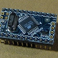
A000003 Arduino, A000003 Datasheet - Page 254

A000003
Manufacturer Part Number
A000003
Description
MCU, MPU & DSP Development Tools MINI
Manufacturer
Arduino
Series
-r
Type
MCUr
Specifications of A000003
Processor To Be Evaluated
Atmega328
Processor Series
ATmega
Data Bus Width
8 bit
Interface Type
USB, RS-232
Operating Supply Voltage
7 V to 9 V
Contents
Board
Lead Free Status / Rohs Status
Lead free / RoHS Compliant
For Use With/related Products
ATmega168
- Current page: 254 of 378
- Download datasheet (8Mb)
23.7
23.8
23.8.1
254
ADC Conversion Result
Register Description
ATmega48/88/168
ADMUX – ADC Multiplexer Selection Register
After the conversion is complete (ADIF is high), the conversion result can be found in the ADC
Result Registers (ADCL, ADCH).
For single ended conversion, the result is
where V
Table 23-2 on page 254
0x3FF represents the selected reference voltage minus one LSB.
• Bit 7:6 – REFS1:0: Reference Selection Bits
These bits select the voltage reference for the ADC, as shown in
changed during a conversion, the change will not go in effect until this conversion is complete
(ADIF in ADCSRA is set). The internal voltage reference options may not be used if an external
reference voltage is being applied to the AREF pin.
Table 23-2.
• Bit 5 – ADLAR: ADC Left Adjust Result
The ADLAR bit affects the presentation of the ADC conversion result in the ADC Data Register.
Write one to ADLAR to left adjust the result. Otherwise, the result is right adjusted. Changing the
ADLAR bit will affect the ADC Data Register immediately, regardless of any ongoing conver-
sions. For a complete description of this bit, see
page
• Bit 4 – Res: Reserved Bit
This bit is an unused bit in the ATmega48/88/168, and will always read as zero.
• Bits 3:0 – MUX3:0: Analog Channel Selection Bits
Bit
(0x7C)
Read/Write
Initial Value
REFS1
0
0
1
1
257.
IN
is the voltage on the selected input pin and V
REFS0
REFS1
Voltage Reference Selections for ADC
R/W
0
1
0
1
7
0
REFS0
Voltage Reference Selection
AREF, Internal V
AV
Reserved
Internal 1.1V Voltage Reference with external capacitor at AREF pin
R/W
6
0
and
CC
with external capacitor at AREF pin
Table 23-3 on page
ADLAR
R/W
5
0
ADC
ref
turned off
R
0
4
–
=
V
--------------------------
MUX3
IN
R/W
“ADCL and ADCH – The ADC Data Register” on
V
3
0
⋅
REF
1024
255). 0x000 represents analog ground, and
MUX2
R/W
REF
2
0
the selected voltage reference (see
MUX1
R/W
1
0
Table
MUX0
R/W
0
0
23-2. If these bits are
ADMUX
2545S–AVR–07/10
Related parts for A000003
Image
Part Number
Description
Manufacturer
Datasheet
Request
R

Part Number:
Description:
Daughter Cards & OEM Boards ARDUINO UNO PROTO PCB REV 3
Manufacturer:
Arduino

Part Number:
Description:
Daughter Cards & OEM Boards ARDUINO SHIELD PROTO KIT REV 3
Manufacturer:
Arduino

Part Number:
Description:
Daughter Cards & OEM Boards ARDUINO MEGA PROTO KIT REV 3
Manufacturer:
Arduino

Part Number:
Description:
Daughter Cards & OEM Boards ARDUINO MEGA PROTO PCB REV 3
Manufacturer:
Arduino

Part Number:
Description:
Development Boards & Kits - AVR ARDUINO STARTER KIT W/ UNO REV3
Manufacturer:
Arduino

Part Number:
Description:
RF Development Tools ARDUINO SHIELD WIRELESS PROTO
Manufacturer:
Arduino
Datasheet:

Part Number:
Description:
RF Development Tools ARDUINO SHIELD WIRELESS WITH SD
Manufacturer:
Arduino
Datasheet:

Part Number:
Description:
Development Software Getting started w/Arduino
Manufacturer:
Arduino

Part Number:
Description:
Ethernet Modules & Development Tools Ethernet Shield for Arduino
Manufacturer:
Arduino

Part Number:
Description:
MCU, MPU & DSP Development Tools LilyPad Arduino Main Board
Manufacturer:
Arduino

Part Number:
Description:
ARDUINO NANO Board
Manufacturer:
Arduino
Datasheet:

Part Number:
Description:
Ethernet Modules & Development Tools ETHERNET SHEILD PoE FOR ARDUINO
Manufacturer:
Arduino
Datasheet:

Part Number:
Description:
ATMEGA328 MCU IC W/ Arduino UNO Bootloader
Manufacturer:
Arduino
Datasheet:

Part Number:
Description:
Memory Cards MICRO SD CARD 1GB WITH SD ADAPTER
Manufacturer:
Arduino


