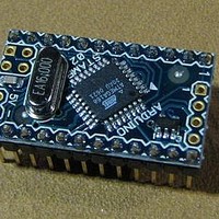
A000003 Arduino, A000003 Datasheet - Page 241
A000003
Manufacturer Part Number
A000003
Description
MCU, MPU & DSP Development Tools MINI
Manufacturer
Arduino
Series
-r
Type
MCUr
Specifications of A000003
Processor To Be Evaluated
Atmega328
Processor Series
ATmega
Data Bus Width
8 bit
Interface Type
USB, RS-232
Operating Supply Voltage
7 V to 9 V
Contents
Board
Lead Free Status / Rohs Status
Lead free / RoHS Compliant
For Use With/related Products
ATmega168


22.3
22.3.1
22.3.2
2545S–AVR–07/10
Register Description
ADCSRB – ADC Control and Status Register B
ACSR – Analog Comparator Control and Status Register
Table 22-1.
• Bit 6 – ACME: Analog Comparator Multiplexer Enable
When this bit is written logic one and the ADC is switched off (ADEN in ADCSRA is zero), the
ADC multiplexer selects the negative input to the Analog Comparator. When this bit is written
logic zero, AIN1 is applied to the negative input of the Analog Comparator. For a detailed
description of this bit, see
• Bit 7 – ACD: Analog Comparator Disable
When this bit is written logic one, the power to the Analog Comparator is switched off. This bit
can be set at any time to turn off the Analog Comparator. This will reduce power consumption in
Active and Idle mode. When changing the ACD bit, the Analog Comparator Interrupt must be
disabled by clearing the ACIE bit in ACSR. Otherwise an interrupt can occur when the bit is
changed.
• Bit 6 – ACBG: Analog Comparator Bandgap Select
When this bit is set, a fixed bandgap reference voltage replaces the positive input to the Analog
Comparator. When this bit is cleared, AIN0 is applied to the positive input of the Analog Compar-
ator. When the bandgap reference voltage is used as input to the Analog Comparator, it will take
a certain time for the voltage to stabilize. If not stabilized, the first conversion may give a wrong
value. See
• Bit 5 – ACO: Analog Comparator Output
The output of the Analog Comparator is synchronized and then directly connected to ACO. The
synchronization introduces a delay of 1 - 2 clock cycles.
Bit
(0x7B)
Read/Write
Initial Value
Bit
0x30 (0x50)
Read/Write
Initial Value
ACME
1
1
1
1
1
1
1
“Internal Voltage Reference” on page 47
Analog Comparator Multiplexed Input (Continued)
ACD
R/W
ADEN
R
7
0
7
–
0
0
0
0
0
0
0
0
ACBG
ACME
R/W
R/W
“Analog Comparator Multiplexed Input” on page
6
0
6
0
MUX2..0
001
010
011
100
101
110
111
ACO
N/A
R
5
R
5
–
0
Analog Comparator Negative Input
ADC1
ADC2
ADC3
ADC4
ADC5
ADC6
ADC7
R/W
ACI
4
0
R
4
–
0
ACIE
R/W
3
0
R
3
–
0
ADTS2
ACIC
R/W
R/W
ATmega48/88/168
2
0
2
0
ADTS1
ACIS1
R/W
R/W
1
0
1
0
240.
ADTS0
ACIS0
R/W
R/W
0
0
0
0
ADCSRB
ACSR
241
Related parts for A000003
Image
Part Number
Description
Manufacturer
Datasheet
Request
R

Part Number:
Description:
Daughter Cards & OEM Boards ARDUINO UNO PROTO PCB REV 3
Manufacturer:
Arduino
Part Number:
Description:
Daughter Cards & OEM Boards ARDUINO SHIELD PROTO KIT REV 3
Manufacturer:
Arduino
Part Number:
Description:
Daughter Cards & OEM Boards ARDUINO MEGA PROTO KIT REV 3
Manufacturer:
Arduino
Part Number:
Description:
Daughter Cards & OEM Boards ARDUINO MEGA PROTO PCB REV 3
Manufacturer:
Arduino
Part Number:
Description:
Development Boards & Kits - AVR ARDUINO STARTER KIT W/ UNO REV3
Manufacturer:
Arduino
Part Number:
Description:
RF Development Tools ARDUINO SHIELD WIRELESS PROTO
Manufacturer:
Arduino
Datasheet:
Part Number:
Description:
RF Development Tools ARDUINO SHIELD WIRELESS WITH SD
Manufacturer:
Arduino
Datasheet:

Part Number:
Description:
Development Software Getting started w/Arduino
Manufacturer:
Arduino

Part Number:
Description:
Ethernet Modules & Development Tools Ethernet Shield for Arduino
Manufacturer:
Arduino

Part Number:
Description:
MCU, MPU & DSP Development Tools LilyPad Arduino Main Board
Manufacturer:
Arduino

Part Number:
Description:
ARDUINO NANO Board
Manufacturer:
Arduino
Datasheet:
Part Number:
Description:
Ethernet Modules & Development Tools ETHERNET SHEILD PoE FOR ARDUINO
Manufacturer:
Arduino
Datasheet:

Part Number:
Description:
ATMEGA328 MCU IC W/ Arduino UNO Bootloader
Manufacturer:
Arduino
Datasheet:
Part Number:
Description:
Memory Cards MICRO SD CARD 1GB WITH SD ADAPTER
Manufacturer:
Arduino