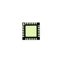
C8051F411-GMR Silicon Laboratories Inc, C8051F411-GMR Datasheet - Page 95

C8051F411-GMR
Manufacturer Part Number
C8051F411-GMR
Description
Microcontrollers (MCU) 50 MIPS 32KB 12ADC RTCLOCK 28 PIN MCU
Manufacturer
Silicon Laboratories Inc
Datasheet
1.C8051F410DK.pdf
(270 pages)
Specifications of C8051F411-GMR
Processor Series
C8051F4x
Core
8051
Data Bus Width
8 bit
Program Memory Type
Flash
Program Memory Size
32 KB
Data Ram Size
2.25 KB
Interface Type
I2C, SMBus, SPI, UART
Maximum Clock Frequency
50 MHz
Number Of Programmable I/os
20
Number Of Timers
4
Maximum Operating Temperature
+ 85 C
Mounting Style
SMD/SMT
Package / Case
QFN
3rd Party Development Tools
PK51, CA51, A51, ULINK2
Development Tools By Supplier
C8051F410DK
Minimum Operating Temperature
- 40 C
On-chip Adc
12 bit, 20 Channel
On-chip Dac
12 bit, 2 Channel
Package
28QFN EP
Device Core
8051
Family Name
C8051F41x
Maximum Speed
50 MHz
Ram Size
2.25 KB
Operating Supply Voltage
1.8|2.5|3.3|5 V
Operating Temperature
-40 to 85 °C
Lead Free Status / Rohs Status
Details
Available stocks
Company
Part Number
Manufacturer
Quantity
Price
Company:
Part Number:
C8051F411-GMR
Manufacturer:
SiliconL
Quantity:
3 000
Part Number:
C8051F411-GMR
Manufacturer:
SILICON LABS/èٹ¯ç§‘
Quantity:
20 000
- Current page: 95 of 270
- Download datasheet (2Mb)
10.1.2. MOVX Instruction and Program Memory
The MOVX instruction is typically used to access data stored in XDATA memory space. In the CIP-51, the
MOVX instruction can also be used to write or erase on-chip program memory space implemented as re-
programmable Flash memory. The Flash access feature provides a mechanism for the CIP-51 to update
program code and use the program memory space for non-volatile data storage. Refer to
“16. Flash Memory” on page 135
ADD A, Rn
ADD A, direct
ADD A, @Ri
ADD A, #data
ADDC A, Rn
ADDC A, direct
ADDC A, @Ri
ADDC A, #data
SUBB A, Rn
SUBB A, direct
SUBB A, @Ri
SUBB A, #data
INC A
INC Rn
INC direct
INC @Ri
DEC A
DEC Rn
DEC direct
DEC @Ri
INC DPTR
MUL AB
DIV AB
DA A
ANL A, Rn
ANL A, direct
ANL A, @Ri
ANL A, #data
ANL direct, A
ANL direct, #data
ORL A, Rn
ORL A, direct
Notes:
1. Assumes PFEN = 1 for all instruction timing.
2. MOVC instructions take 4 to 7 clock cycles depending on instruction alignment and the FLRT setting (SFR
Definition 16.3. FLSCL: Flash Scale).
Mnemonic
Table 10.1. CIP-51 Instruction Set Summary
Add register to A
Add direct byte to A
Add indirect RAM to A
Add immediate to A
Add register to A with carry
Add direct byte to A with carry
Add indirect RAM to A with carry
Add immediate to A with carry
Subtract register from A with borrow
Subtract direct byte from A with borrow
Subtract indirect RAM from A with borrow
Subtract immediate from A with borrow
Increment A
Increment register
Increment direct byte
Increment indirect RAM
Decrement A
Decrement register
Decrement direct byte
Decrement indirect RAM
Increment Data Pointer
Multiply A and B
Divide A by B
Decimal adjust A
AND Register to A
AND direct byte to A
AND indirect RAM to A
AND immediate to A
AND A to direct byte
AND immediate to direct byte
OR Register to A
OR direct byte to A
for further details.
Arithmetic Operations
Logical Operations
Rev. 1.1
Description
C8051F410/1/2/3
1
Bytes
1
2
1
2
1
2
1
2
1
2
1
2
1
1
2
1
1
1
2
1
1
1
1
1
1
2
1
2
2
3
1
2
Cycles
Clock
Section
1
2
2
2
1
2
2
2
1
2
2
2
1
1
2
2
1
1
2
2
1
4
8
1
1
2
2
2
2
3
1
2
95
Related parts for C8051F411-GMR
Image
Part Number
Description
Manufacturer
Datasheet
Request
R
Part Number:
Description:
SMD/C°/SINGLE-ENDED OUTPUT SILICON OSCILLATOR
Manufacturer:
Silicon Laboratories Inc
Part Number:
Description:
Manufacturer:
Silicon Laboratories Inc
Datasheet:
Part Number:
Description:
N/A N/A/SI4010 AES KEYFOB DEMO WITH LCD RX
Manufacturer:
Silicon Laboratories Inc
Datasheet:
Part Number:
Description:
N/A N/A/SI4010 SIMPLIFIED KEY FOB DEMO WITH LED RX
Manufacturer:
Silicon Laboratories Inc
Datasheet:
Part Number:
Description:
N/A/-40 TO 85 OC/EZLINK MODULE; F930/4432 HIGH BAND (REV E/B1)
Manufacturer:
Silicon Laboratories Inc
Part Number:
Description:
EZLink Module; F930/4432 Low Band (rev e/B1)
Manufacturer:
Silicon Laboratories Inc
Part Number:
Description:
I°/4460 10 DBM RADIO TEST CARD 434 MHZ
Manufacturer:
Silicon Laboratories Inc
Part Number:
Description:
I°/4461 14 DBM RADIO TEST CARD 868 MHZ
Manufacturer:
Silicon Laboratories Inc
Part Number:
Description:
I°/4463 20 DBM RFSWITCH RADIO TEST CARD 460 MHZ
Manufacturer:
Silicon Laboratories Inc
Part Number:
Description:
I°/4463 20 DBM RADIO TEST CARD 868 MHZ
Manufacturer:
Silicon Laboratories Inc
Part Number:
Description:
I°/4463 27 DBM RADIO TEST CARD 868 MHZ
Manufacturer:
Silicon Laboratories Inc
Part Number:
Description:
I°/4463 SKYWORKS 30 DBM RADIO TEST CARD 915 MHZ
Manufacturer:
Silicon Laboratories Inc
Part Number:
Description:
N/A N/A/-40 TO 85 OC/4463 RFMD 30 DBM RADIO TEST CARD 915 MHZ
Manufacturer:
Silicon Laboratories Inc
Part Number:
Description:
I°/4463 20 DBM RADIO TEST CARD 169 MHZ
Manufacturer:
Silicon Laboratories Inc


