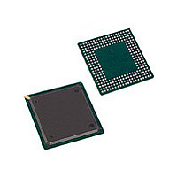
PI7C8150BND Pericom Semiconductor, PI7C8150BND Datasheet - Page 100

PI7C8150BND
Manufacturer Part Number
PI7C8150BND
Description
Manufacturer
Pericom Semiconductor
Datasheet
1.PI7C8150BND.pdf
(106 pages)
Specifications of PI7C8150BND
Operating Temperature (min)
0C
Operating Temperature Classification
Commercial
Operating Temperature (max)
85C
Package Type
BGA
Rad Hardened
No
Lead Free Status / Rohs Status
Not Compliant
Available stocks
Company
Part Number
Manufacturer
Quantity
Price
Company:
Part Number:
PI7C8150BNDE
Manufacturer:
CYPRESS
Quantity:
101
Part Number:
PI7C8150BNDE
Manufacturer:
PERICOM
Quantity:
20 000
Company:
Part Number:
PI7C8150BNDIE
Manufacturer:
PERICOM
Quantity:
300
Company:
Part Number:
PI7C8150BNDIE
Manufacturer:
PERICOM
Quantity:
301
Part Number:
PI7C8150BNDIE
Manufacturer:
PERICOM
Quantity:
20 000
17
17.1
17.2
ELECTRICAL AND TIMING SPECIFICATIONS
MAXIMUM RATINGS
(Above which the useful life may be impaired. For user guidelines, not tested).
Note:
Stresses greater than those listed under MAXIMUM RATINGS may cause permanent
damage to the device. This is a stress rating only and functional operation of the device at
these or any conditions above those indicated in the operational sections of this
specification is not implied. Exposure to absolute maximum rating conditions for extended
periods of time may affect reliability.
DC SPECIFICATIONS
Notes:
1. CMOS Input pins: S_CFN_L, TCK, TMS, TDI, TRST_L, SCAN_EN, SCAN_TM_L
2. CMOS Output pin: TDO
3. PCI pins: P_AD[31:0], P_CBE[3:0], P_PAR, P_FRAME_L, P_IRDY_L, P_TRDY_L,
P_DEVSEL_L, P_STOP_L, P_LOCK_L, PIDSEL_L, P_PERR_L, P_SERR_L,
P_REQ_L, P_GNT_L, P_RESET_L, S_AD[31:0], S_CBE[3:0], S_PAR, S_FRAME_L,
S_IRDY_L, S_TRDY_L, S_DEVSEL_L, S_STOP_L, S_LOCK_L, S_PERR_L,
S_SERR_L, S_REQ[7:0]_L, S_GNT[7:0]_L, S_RESET_L, S_EN, HSLED, HS_SW_L,
HS_EN, ENUM_L.
4. V
Storage Temperature
Ambient Temperature with Power Applied
Supply Voltage to Ground Potentials (AV
Voltage at Input Pins
Symbol
V
AV
V
V
V
V
V
I
V
V
V
V
C
C
C
L
il
pin
in
CLK
IDSEL
DD
ih
il
ih
il
ipu
oh
ol
oh
ol
CC
,
DD
is in reference to the V
Parameter
Supply Voltage
Input HIGH Voltage
Input LOW Voltage
CMOS Input HIGH Voltage
CMOS Input LOW Voltage
Input Pull-up Voltage
Input Leakage Current
Output HIGH Voltage
Output LOW Voltage
CMOS Output HIGH Voltage
CMOS Output LOW Voltage
Input Pin Capacitance
CLK Pin Capacitance
IDSEL Pin Capacitance
Pin Inductance
DD
of the input device.
CC
90
and V
Condition
0 < V
I
I
I
I
out
out
out
out
DD
= -500µA
= 1500µA
= -500µA
= 1500µA
only]
in
< V
DD
March 19, 2003 – Revision 1.04
Min.
3
0.5 V
-0.5
0.7 V
-0.5
0.7 V
0.9V
V
5
2-PORT PCI-TO-PCI BRIDGE
DD
ADVANCE INFORMATION
– 0.5
DD
DD
DD
DD
-65°C to 150°C
0°C to 85°C
-0.3V to 3.6V
-0.5V to 5.5V
Max.
3.6
V
0.3 V
V
0.3 V
±10
0.1 V
0.5
10
12
8
20
DD
DD
+ 0.5
+ 0.5
DD
DD
DD
PI7C8150
Units
V
V
V
V
V
V
µA
V
V
V
V
pF
pF
pF
nH
Notes
3, 4
3, 4
1, 4
1, 4
3
3
3
3
2
2
3
3
3
3


