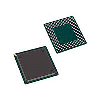
PI7C8150BND Pericom Semiconductor, PI7C8150BND Datasheet - Page 94

PI7C8150BND
Manufacturer Part Number
PI7C8150BND
Description
Manufacturer
Pericom Semiconductor
Datasheet
1.PI7C8150BND.pdf
(106 pages)
Specifications of PI7C8150BND
Operating Temperature (min)
0C
Operating Temperature Classification
Commercial
Operating Temperature (max)
85C
Package Type
BGA
Rad Hardened
No
Lead Free Status / Rohs Status
Not Compliant
Available stocks
Company
Part Number
Manufacturer
Quantity
Price
Company:
Part Number:
PI7C8150BNDE
Manufacturer:
CYPRESS
Quantity:
101
Part Number:
PI7C8150BNDE
Manufacturer:
PERICOM
Quantity:
20 000
Company:
Part Number:
PI7C8150BNDIE
Manufacturer:
PERICOM
Quantity:
300
Company:
Part Number:
PI7C8150BNDIE
Manufacturer:
PERICOM
Quantity:
301
Part Number:
PI7C8150BNDIE
Manufacturer:
PERICOM
Quantity:
20 000
16.1.1
16.1.2
that allows all processor signal pins to be driven and/or sampled, thereby providing direct
control and monitoring of processor pins at the system level.
This mode of operation is valuable for design debugging and fault diagnosis since it
permits examination of connections not normally accessible to the test system. The
following subsections describe the boundary-scan test logic elements: TAP pins,
instruction register, test data registers and TAP controller. Figure 16-1 illustrates how these
pieces fit together to form the JTAG unit.
TAP PINS
The PI7C8150’s TAP pins form a serial port composed of four input connections (TMS,
TCK, TRST_L and TDI) and one output connection (TDO). These pins are described in
Table 16-1. The TAP pins provide access to the instruction register and the test data
registers.
INSTRUCTION REGISTER
The Instruction Register (IR) holds instruction codes. These codes are shifted in through
the Test Data Input (TDI) pin. The instruction codes are used to select the specific test
operation to be performed and the test data register to be accessed.
The instruction register is a parallel-loadable, master/slave-configured 5-bit wide, serial-
shift register with latched outputs. Data is shifted into and out of the IR serially through the
TDI pin clocked by the rising edge of TCK. The shifted-in instruction becomes active upon
latching from the master stage to the slave stage. At that time the IR outputs along with the
TAP finite state machine outputs are decoded to select and control the test data register
selected by that instruction. Upon latching, all actions caused by any previous instructions
terminate.
Figure 16-1. Test Access Port Block Diagram
84
March 19, 2003 – Revision 1.04
2-PORT PCI-TO-PCI BRIDGE
ADVANCE INFORMATION
PI7C8150


