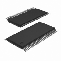
SC28L202A1DGG/G,11 NXP Semiconductors, SC28L202A1DGG/G,11 Datasheet - Page 10

SC28L202A1DGG/G,11
Manufacturer Part Number
SC28L202A1DGG/G,11
Description
IC UART DUAL W/FIFO 56-TSSOP
Manufacturer
NXP Semiconductors
Series
IMPACTr
Datasheet
1.SC28L202A1DGG118.pdf
(77 pages)
Specifications of SC28L202A1DGG/G,11
Features
False-start Bit Detection
Number Of Channels
2, DUART
Fifo's
256 Byte
Voltage - Supply
3.3V, 5V
With Parallel Port
Yes
With Auto Flow Control
Yes
With False Start Bit Detection
Yes
With Modem Control
Yes
With Cmos
Yes
Mounting Type
Surface Mount
Package / Case
56-TFSOP (0.240", 6.10mm Width)
Lead Free Status / RoHS Status
Lead free / RoHS Compliant
Other names
935279792118
SC28L202A1DGG/G-T
SC28L202A1DGG/G-T
SC28L202A1DGG/G-T
SC28L202A1DGG/G-T
Philips Semiconductors
CONFIGURATION FOR 68XXX BUS INTERFACE (MOTOROLA) (see Figure 2)
2005 Nov 01
Symbol
I/M
D0–D7
CEN
R/WN
IACKN
DACKN
A6–A0
RESETN
IRQN
X1/SCLK
X2
RxD A
RxD B
TxD A
TxD B
I/O[7:0]A
I/O[7:0]B
Vcc
Vss
n.c.
Dual UART
Pin no.
21
20–17,
12–9
29
30
26
31
3–6,
23–25
8
54
55
56
7
22
53
32
45–52
33–40
1, 13,
27, 41,
42
2, 15,
16, 28,
43, 44
14
Pin
type
I
I/O
I
I
I
O
I
I
O
I
O
I
I
O
O
I/O
I/O
Power
Power
Name and Function
Bus Configuration: When LOW configures the bus interface to the Conditions shown in this table.
Data Bus: Bi-directional 3-State data bus used to transfer commands, data and status between the DUART and
the CPU. D0 is the least significant bit.
Chip Enable: Active-LOW input signal. When LOW, data transfers between the CPU and the DUART are
enabled on D0–D7 as controlled by the R/WN and A0–A6 inputs. When HIGH, places the D0–D7 lines in the
3-State condition.
Read/Write: Input Signal. When CEN is LOW R/WN HIGH input a read cycle, when LOW a write cycle.
Interrupt Acknowledge: Active-LOW input indicates an interrupt acknowledge cycle. Usually asserted by the
CPU in response to an interrupt request. When asserted places the interrupt vector on the bus and asserts
DACKN.
Data Transfer Acknowledge: An open-drain active-LOW output asserted in a write, read, or interrupt
acknowledge cycle to indicate proper transfer of data between the CPU and the DUART.
Address Inputs: Select the DUART internal registers and ports for read/write operations.
Reset: A LOW level clears internal registers (SR A , SR B, IMR, ISR, OPR, OPCR), places I/O[7:0] A and B at
high impedance input state, stops the counter/timer, and puts Channels A and B in the inactive state, with the
TxD A and TxD B outputs in the mark (HIGH) state. Sets MR pointer to MR1, 9600 baud, 1 start, no parity and
1 stop bit(s). (See Reset Table)
Interrupt Request: Active-LOW, open-drain, output which signals the CPU that one or more of the eighteen (18)
maskable interrupting conditions are true.
Crystal 1: Crystal or external clock input. A crystal or clock of the specified limits must be supplied at all times.
When a crystal is used, a capacitor must be connected from this pin to ground (see Figure 12).
Crystal 2: Connection for other side of the crystal. When a crystal is used, a capacitor must be connected from
this pin to ground (see Figure 12). If Sclk is driven from an external source, this pin must be left open.
Channel A Receiver Serial Data Input: The least significant bit is received first. ‘Mark’ is HIGH; ‘space’ is LOW.
Channel B Receiver Serial Data Input: The least significant bit is received first. ‘Mark’ is HIGH; ‘space’ is LOW.
Channel A Transmitter Serial Data Output: The least significant bit is transmitted first. This output is held in
the ‘mark’ condition when the transmitter is disabled, idle or when operating in local loop back mode.
‘Mark’ is HIGH; ‘space’ is LOW.
Channel B Transmitter Serial Data Output: The least significant bit is transmitted first. This output is held in
the ‘mark’ condition when the transmitter is disabled, idle, or when operating in local loop back mode. ‘Mark’ is
HIGH; ‘space’ is LOW.
General-purpose input and output ports channel A: The character of these pins is controlled by I/OPCR.
They may be inputs or outputs and will present many internal clocks and interrupt signals: RTS, CTS, DTR, DSR
etc. All have change of state detectors and the input is always active. These pins are set to input only when
addressed from the low order 16 address space. When these pins are configured for interrupt type signals
(RxRDY, TxRDY, C/TRDY) They switch to open drain outputs. Each of these pins have a small pull-up ‘resistor’
that supplies approximately 5 A of current.
General-purpose input and output ports channel B: The character of these pins is controlled by I/OPCR.
They may be inputs or outputs and will present many internal clocks and interrupt signals: RTS, CTS, DTR, DSR
etc. All have change of state detectors and the input is always active. These pins are set to output only when
addressed from the low order 16 address space. When these pins are configured for interrupt type signals
(RxRDY, TxRDY, C/TRDY) They switch to open drain outputs. Each of these pins have a small pull-up ‘resistor’
that supplies approximately 5 A of current.
Power Supply (5 pins): +3.3 or +5V supply input
5.5 V. Timing parameters are specified with respect to the Vcc being at 3.3 V
Ground (6 Vss Pins)
not connected
4
10% (4 Vcc Pins) ). Operation is assured from 2.97 V to
10% or 5.0 V
SC28L202
Product data sheet
10%.


