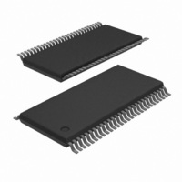
SC28L202A1DGG/G,11 NXP Semiconductors, SC28L202A1DGG/G,11 Datasheet - Page 66

SC28L202A1DGG/G,11
Manufacturer Part Number
SC28L202A1DGG/G,11
Description
IC UART DUAL W/FIFO 56-TSSOP
Manufacturer
NXP Semiconductors
Series
IMPACTr
Datasheet
1.SC28L202A1DGG118.pdf
(77 pages)
Specifications of SC28L202A1DGG/G,11
Features
False-start Bit Detection
Number Of Channels
2, DUART
Fifo's
256 Byte
Voltage - Supply
3.3V, 5V
With Parallel Port
Yes
With Auto Flow Control
Yes
With False Start Bit Detection
Yes
With Modem Control
Yes
With Cmos
Yes
Mounting Type
Surface Mount
Package / Case
56-TFSOP (0.240", 6.10mm Width)
Lead Free Status / RoHS Status
Lead free / RoHS Compliant
Other names
935279792118
SC28L202A1DGG/G-T
SC28L202A1DGG/G-T
SC28L202A1DGG/G-T
SC28L202A1DGG/G-T
1. Parameters are valid over specified temperature range.
2. All voltage measurements are referenced to ground (GND). For testing, all inputs swing between 0.4 V and 3.0 V with a transition time of
3. Test conditions for outputs: C
4. Typical values are at +25 C, typical supply voltages, and typical processing parameters.
5. Timing is illustrated and referenced to the WRN and RDN inputs. Also, CEN may be the ‘strobing’ input. CEN and RDN (also CEN and
6. Guaranteed by characterization of sample units.
7. If CEN is used as the ‘strobing’ input, the parameter defines the minimum High times between one CEN and the next. The RDN signal must
8. Minimum frequencies are not tested but are guaranteed by design.
9. Clocks for 1X mode should be reasonably symmetrical.
10. Data is usually set up with respect to CEN going LOW—the leading edge of CEN. This mode strongly implies the use of DACKN. (Its use is
Philips Semiconductors
NOTES:
TIMING DIAGRAMS
The active time of read or write cycle exists only when CEN is LOW
and RDN or CEN is also LOW.
Write = CEN and WRN LOW.
Read = CEN and RDN LOW.
For the 68K mode:
Write = CEN LOW and RWN LOW and DACKN HIGH.
Read = CEN LOW and RWN HIGH.
In general, it is convenient (but is not at all required) to think of the
Read/Write signal to be active and then let the CEN be the ‘strobing’
or clocking control. However, some users have wired CEN LOW and
allowed RDN or WRN to be the clocking or ‘strobing’ input. While
this is completely within the specified limits, it is not recommended
since it will greatly increase the part’s sensitivity to noise ‘glitches’
on the RDN and WRN signals.
2005 Nov 01
Symbol
68000 or Motorola bus timing (See Figures 7, 8, 9)
t
t
t
t
t
t
t
t
T
t
t
CS(mot)
DS(mot)
DH(mot)
AS(mot)
AH(mot)
DD(mot)
RWD(mot)
DCR
DAT
CSC
DCW
Dual UART
5 ns maximum. For X1/SCLK this swing is between 0.4 V and 4.4 V. All time measurements are referenced at input voltages of 0.8 V and
2.0 V and output voltages of 0.8 V and 2.0 V, as appropriate.
WRN) are ORed internally. The signal asserted last initiates the cycle and the signal negated first terminates the cycle.
be negated for t
not strictly required.) DACKN is derived from the X1/SCLK input. It is seldom that the system clocks that ultimately drive the CEN, address
and RWN signals are synchronous to the X1/SCLK. If address, data, RWN are set up before CEN goes LOW and hold through DACKN, the
timing parameters above will be guaranteed.
Parameter
RWN set-up time to CEN LOW
Data bus set-up time before X1 HIGH
Data hold time after CEN HIGH
Address set-up time to CEN LOW
Address hold time from CEN LOW
Data valid after CEN LOW
HIGH time between read and/or write cycles
DACKN Low (read cycle) from X1 High
DACKN Low (write cycle) from X1 High
DACKN High impedance from CEN or IACKN high
CEN or IACKN set-up time to X1 high for minimum DACKN cycle
RWD
time to guarantee that any status register changes are valid.
L
= 85 pF, except interrupt outputs. Test conditions for interrupt outputs: C
5, 7
60
For the 68K mode, the CEN is very much the clock or ‘strobing’
signal. The RDN and WRN signals have been combined into the
RWN signal. Therefore, the part is always prepared to do a write or
read—it only needs CEN to enable.
In the 68K mode design, care should be given to system drift over
temperature, voltage, and age when RWN and CEN change very
close to each other. If RWN switches shortly before CEN (due to
system drift) it is possible to produce very short internal read or write
pulses which could change internal controls, FIFO address pointers,
for example.
Figure 3 loosely shows the timing conditions that may exist of the
active area those signals will produce.
LIMITS
Min
5
10
0
10
10
–
10
–
–
–
10
L
= 85 pF, R
4
Typ
–
–
–
–
–
–
–
–
–
–
–
L
= 2.7 k to V
SC28L202
–
–
–
–
–
45
–
35
30
15
–
Max
Product data sheet
CC
UNIT
ns
ns
ns
ns
ns
ns
ns
ns
ns
ns
ns
.


