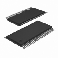
SC28L202A1DGG/G,11 NXP Semiconductors, SC28L202A1DGG/G,11 Datasheet - Page 54

SC28L202A1DGG/G,11
Manufacturer Part Number
SC28L202A1DGG/G,11
Description
IC UART DUAL W/FIFO 56-TSSOP
Manufacturer
NXP Semiconductors
Series
IMPACTr
Datasheet
1.SC28L202A1DGG118.pdf
(77 pages)
Specifications of SC28L202A1DGG/G,11
Features
False-start Bit Detection
Number Of Channels
2, DUART
Fifo's
256 Byte
Voltage - Supply
3.3V, 5V
With Parallel Port
Yes
With Auto Flow Control
Yes
With False Start Bit Detection
Yes
With Modem Control
Yes
With Cmos
Yes
Mounting Type
Surface Mount
Package / Case
56-TFSOP (0.240", 6.10mm Width)
Lead Free Status / RoHS Status
Lead free / RoHS Compliant
Other names
935279792118
SC28L202A1DGG/G-T
SC28L202A1DGG/G-T
SC28L202A1DGG/G-T
SC28L202A1DGG/G-T
Philips Semiconductors
IMR – Interrupt Mask Register
The programming of this register selects which bits in the ISR causes an interrupt output. If a bit in the ISR is a ‘1’ and the corresponding bit in
the IMR is also a ‘1’ the INTRN output will be asserted. If the corresponding bit in the IMR is a zero, the state of the bit in the ISR has no effect
on the INTRN output. Note that the IMR does not mask the programmable interrupt outputs I/O3 B–I/O7 B or the reading of the ISR.
CTPU Counter Timer Preset Upper (Counter/Timer 0)
CTPL Counter –Timer Preset Lower (Counter/Timer 0)
CTVU Counter Timer Value Upper (Counter/Timer 0)
CTVL Counter –Timer Value Lower (Counter/Timer 0)
Only the counter/timer 0 is available in the low order 16–position address map. Issuing the start command loads the C/T with the preset value.
The Stop command resets the C/T ready bit in the ISR (Interrupt status Register) and captures the C/T value in the output latches of the C/T. In
the special time out mode the start and stop commands are ignored. The ‘start command is executed by a read at address 0xE; the stop at 0xF.
IVR Interrupt Vector register in 68K mode and General purpose read write register in the x86 mode
IPR Input Port Register I/O(6:0) A
2005 Nov 01
IMR
CPTU
CTPL
CPVL
CTVL
IVR
IPR
Dual UART
Bit 7
The upper eight (8) bits for the 16 bit counter timer preset register
Bit 7
The lower eight (8) bits for the 16 bit counter timer preset register
Bit 7
The lower eight (8) bits for the 16 bit counter timer value
Bit 7
The lower eight (8) bits for the 16 bit counter timer value register
Bit 7
The eight (8) bits of the interrupt vector in the 68K mode.
Bit 7
Logical levels or the I/O[6:0] A, Bit 7 read as ‘1’
Bit 7
INPUT PORT
CHANGE
0=not
enabled
1=enabled
BIT 6
BIT 6
BIT 6
BIT 6
BIT 6
BIT 6
BIT 6
Delta
Break B
0=not
enabled
1=enabled
BIT 5
BIT 5
BIT 5
BIT 5
BIT 5
BIT 5
BIT 5
RxRDY/
FFULL B
0=not
enabled
1=enabled
BIT 4
BIT 4
BIT 4
BIT 4
BIT 4
BIT 4
BIT 4
TxRDY B
0=not
enabled
1=enabled
48
BIT 3
BIT 3
BIT 3
BIT 3
BIT 3
BIT 3
Counter
Ready
0=not
enabled
1=enabled
BIT 3
BIT 2
BIT 2
BIT 2
BIT 2
BIT 2
BIT 2
Delta
Break A
0=not
enabled
1=enabled
BIT 2
BIT 1
BIT 1
BIT 1
BIT 1
BIT 1
BIT 1
RxRDY/
FFULL A
0=not
enabled
1=enabled
BIT 1
SC28L202
Product data sheet
BIT 0
BIT 0
BIT 0
BIT 0
BIT 0
BIT 0
TxRDY A
0=not
enabled
1=enabled
BIT 0


