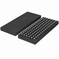
SSTU32864EC/G,551 NXP Semiconductors, SSTU32864EC/G,551 Datasheet - Page 19

SSTU32864EC/G,551
Manufacturer Part Number
SSTU32864EC/G,551
Description
IC BUFFER 1.8V 25BIT SOT536-1
Manufacturer
NXP Semiconductors
Datasheet
1.SSTU32864ECG557.pdf
(21 pages)
Specifications of SSTU32864EC/G,551
Logic Type
1:1, 1:2 Configurable Registered Buffer
Supply Voltage
1.7 V ~ 1.9 V
Number Of Bits
25, 14
Operating Temperature
0°C ~ 70°C
Mounting Type
Surface Mount
Package / Case
96-LFBGA
Logic Family
SSTU
Logical Function
Registered Buffer
Number Of Elements
1
Number Of Inputs
25
Number Of Outputs
25
High Level Output Current
-8mA
Low Level Output Current
8mA
Propagation Delay Time
3ns
Operating Supply Voltage (typ)
1.8V
Operating Supply Voltage (max)
1.9V
Operating Supply Voltage (min)
1.7V
Clock-edge Trigger Type
Posit/Negat-Edge
Polarity
Non-Inverting
Technology
CMOS
Frequency (max)
450(Min)MHz
Mounting
Surface Mount
Pin Count
96
Operating Temp Range
0C to 70C
Operating Temperature Classification
Commercial
Lead Free Status / RoHS Status
Lead free / RoHS Compliant
Other names
935275429551
SSTU32864EC/G-S
SSTU32864EC/G-S
SSTU32864EC/G-S
SSTU32864EC/G-S
Philips Semiconductors
14. Revision history
Table 12:
9397 750 14092
Product data sheet
Document ID
SSTU32864_2
Modifications:
SSTU32864-01
Revision history
Release date
20041022
20040712
•
•
•
•
•
•
•
•
•
•
•
•
The format of this data sheet has been redesigned to comply with the new presentation and
information standard of Philips Semiconductors.
Data sheet status changed to ‘Product data sheet’.
Table 2 “Pin description”
– (new) Table note [1] added
– pin (ball) numbers added
– changed pin name ‘DNU’ to ‘d.n.u.’
Table 3 “Function table (each flip-flop)”
– moved to
– added
– corrected column sub-headings under ‘Outputs’
Table 4 “Limiting values
Table 5 “Operating
– changed V
– changed V
– Table note split into 2 notes; references added.
Table 6 “Characteristics”
– changed I
Table 7 “Timing
– changed symbol f
– changed symbol t
– changed symbol t
Table 8 “Switching
– changed t
– changed t
Table 9 “Output edge
Section 10.1 “Test
Added
per MHz ...”; change Unit from “ A/MHz” to “ A”.
Section 13 “Abbreviations”
Table note 1
Data sheet status
Product data sheet
Objective data
Section 6.1 on page 7
DDD
PDM
PHL
IH
IL
requirements”:
(for data inputs) to V
(for data inputs) to V
Condition from ‘reset to output’ to ‘RESET to output’
Parameter from “dynamic operating current ...” to “dynamic operating current
and t
1.8 V configurable registered buffer for DDR2 RDIMM applications
circuit”: titles for
characteristics”:
conditions”:
CLOCK
SU
H
rates”: deleted Table note [1]
Rev. 02 — 22 October 2004
PDMSS
to t
and its reference at ‘Outputs’
[1]
to t
”: Symbol V
h
su
to f
Conditions from ‘clock to output’ to ‘CK and CK to output’
clock
Figure 10
IL(AC)
IH(AC)
Change notice
-
-
i
changed to V
and V
and V
and
IL(DC)
IH(DC)
Figure 11
I
; Symbol V
; condition changed to ‘data inputs (Dn)’
; condition changed to ‘data inputs (Dn)’
Doc. number
9397 750 14092
9397 750 13339
modified.
© Koninklijke Philips Electronics N.V. 2004. All rights reserved.
o
changed to V
SSTU32864
Supersedes
SSTU32864-01
-
O
19 of 21


