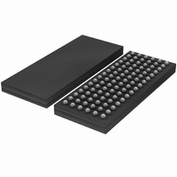
SSTU32864EC/G,551 NXP Semiconductors, SSTU32864EC/G,551 Datasheet

SSTU32864EC/G,551
Specifications of SSTU32864EC/G,551
SSTU32864EC/G-S
SSTU32864EC/G-S
Related parts for SSTU32864EC/G,551
SSTU32864EC/G,551 Summary of contents
Page 1
SSTU32864 1.8 V configurable registered buffer for DDR2 RDIMM applications Rev. 02 — 22 October 2004 1. General description The SSTU32864 is a 25-bit 1:1 or 14-bit 1:2 configurable registered buffer designed for 1 1 All ...
Page 2
Philips Semiconductors 2. Features Configurable register supporting DDR2 Registered DIMM applications Configurable to 25-bit 1:1 mode or 14-bit 1:2 mode Controlled output impedance drivers enable optimal signal integrity and speed Exceeds JESD82-7 speed performance (1.8 ns max. single-bit switching propagation ...
Page 3
Philips Semiconductors 4. Functional diagram (1) Disabled in 1:1 configuration. Fig 1. Functional diagram of SSTU32864; 1:2 mode (positive logic) 9397 750 14092 Product data sheet 1.8 V configurable registered buffer for DDR2 RDIMM applications RESET REF ...
Page 4
Philips Semiconductors 5. Pinning information 5.1 Pinning Fig 2. Pin configuration for LFBGA96 Fig 3. Ball mapping; 1:1 register ( 0); top view 9397 750 14092 Product data sheet 1.8 V configurable registered buffer for DDR2 ...
Page 5
Philips Semiconductors Fig 4. Ball mapping; 1:2 register A ( 1); top view Fig 5. Ball mapping; 1:2 register B ( 1); top view 9397 750 14092 Product data sheet 1.8 V ...
Page 6
Philips Semiconductors 5.2 Pin description Table 2: Pin description Symbol Pin GND B3, B4, D3, D4, F3, F4, H3, H4, K3, K4, M3, M4, P3 A4, C3, C4, E3, DD E4, G3, G4, J3, J4, L3, L4, N3, ...
Page 7
Philips Semiconductors Data outputs = Q10, Q12, Q13 when and Functional description 6.1 Function table Table 3: RESET ...
Page 8
Philips Semiconductors 7. Limiting values [1] Table 4: Limiting values In accordance with the Absolute Maximum Rating System (IEC 60134). Symbol Parameter V supply voltage DD V receiver input voltage I V driver output voltage O I input clamp current ...
Page 9
Philips Semiconductors 8. Recommended operating conditions Table 5: Operating conditions Symbol Parameter V supply voltage DD V reference voltage REF V termination voltage TT V input voltage HIGH-level input voltage data inputs (Dn), IH(AC LOW-level ...
Page 10
Philips Semiconductors 9. Characteristics Table 6: Characteristics Recommended operating conditions, unless otherwise specified. Voltages are referenced to GND (ground = 0 V +70 C. amb Symbol Parameter V HIGH-level output voltage OH V LOW-level output ...
Page 11
Philips Semiconductors Table 7: Timing requirements Recommended operating conditions; V See Figure 6 through Figure 11. Symbol Parameter f clock frequency clock t pulse duration, CK, CK HIGH or W LOW t differential inputs active time ACT t differential inputs ...
Page 12
Philips Semiconductors 10. Test information 10.1 Test circuit All input pulses are supplied by generators having the following characteristics: PRR 10 MHz; Z The outputs are measured one at a time with one transition per measurement. CK inputs (1) C ...
Page 13
Philips Semiconductors Fig 9. Voltage waveforms; set-up and hold times Fig 10. Voltage waveforms; propagation delay times (clock to output) Fig 11. Voltage waveforms; propagation delay times (reset to output) 9397 750 14092 Product data sheet 1.8 V configurable registered ...
Page 14
Philips Semiconductors 10.2 Output slew rate measurement All input pulses are supplied by generators having the following characteristics: PRR 10 MHz; Z (1) C Fig 12. Load circuit, HIGH-to-LOW slew measurement Fig 13. Voltage waveforms, ...
Page 15
Philips Semiconductors 11. Package outline LFBGA96: plastic low profile fine-pitch ball grid array package; 96 balls; body 13.5 x 5.5 x 1.05 mm ball A1 index area ...
Page 16
Philips Semiconductors 12. Soldering 12.1 Introduction to soldering surface mount packages This text gives a very brief insight to a complex technology. A more in-depth account of soldering ICs can be found in our Data Handbook IC26; Integrated Circuit Packages ...
Page 17
Philips Semiconductors – smaller than 1.27 mm, the footprint longitudinal axis must be parallel to the transport direction of the printed-circuit board. The footprint must incorporate solder thieves at the downstream end. • For packages with leads on four sides, ...
Page 18
Philips Semiconductors [4] These packages are not suitable for wave soldering. On versions with the heatsink on the bottom side, the solder cannot penetrate between the printed-circuit board and the heatsink. On versions with the heatsink on the top side, ...
Page 19
Philips Semiconductors 14. Revision history Table 12: Revision history Document ID Release date SSTU32864_2 20041022 • Modifications: The format of this data sheet has been redesigned to comply with the new presentation and information standard of Philips Semiconductors. • Data ...
Page 20
Philips Semiconductors 15. Data sheet status [1] Level Data sheet status Product status I Objective data Development II Preliminary data Qualification III Product data Production [1] Please consult the most recently issued data sheet before initiating or completing a design. ...
Page 21
Philips Semiconductors 19. Contents 1 General description . . . . . . . . . . . . . . . . . . . . . . 1 2 Features . . . . . . . . ...


