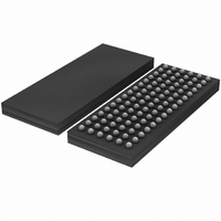
SSTU32864EC/G,551 NXP Semiconductors, SSTU32864EC/G,551 Datasheet - Page 8

SSTU32864EC/G,551
Manufacturer Part Number
SSTU32864EC/G,551
Description
IC BUFFER 1.8V 25BIT SOT536-1
Manufacturer
NXP Semiconductors
Datasheet
1.SSTU32864ECG557.pdf
(21 pages)
Specifications of SSTU32864EC/G,551
Logic Type
1:1, 1:2 Configurable Registered Buffer
Supply Voltage
1.7 V ~ 1.9 V
Number Of Bits
25, 14
Operating Temperature
0°C ~ 70°C
Mounting Type
Surface Mount
Package / Case
96-LFBGA
Logic Family
SSTU
Logical Function
Registered Buffer
Number Of Elements
1
Number Of Inputs
25
Number Of Outputs
25
High Level Output Current
-8mA
Low Level Output Current
8mA
Propagation Delay Time
3ns
Operating Supply Voltage (typ)
1.8V
Operating Supply Voltage (max)
1.9V
Operating Supply Voltage (min)
1.7V
Clock-edge Trigger Type
Posit/Negat-Edge
Polarity
Non-Inverting
Technology
CMOS
Frequency (max)
450(Min)MHz
Mounting
Surface Mount
Pin Count
96
Operating Temp Range
0C to 70C
Operating Temperature Classification
Commercial
Lead Free Status / RoHS Status
Lead free / RoHS Compliant
Other names
935275429551
SSTU32864EC/G-S
SSTU32864EC/G-S
SSTU32864EC/G-S
SSTU32864EC/G-S
Philips Semiconductors
7. Limiting values
Table 4:
In accordance with the Absolute Maximum Rating System (IEC 60134).
[1]
[2]
[3]
9397 750 14092
Product data sheet
Symbol
V
V
V
I
I
I
I
T
IK
OK
O
CCC
stg
DD
I
O
Stresses beyond those listed under ‘absolute maximum ratings’ may cause permanent damage to the device. These are stress ratings
only and functional operation of the device at these or any other conditions beyond those indicated under ‘recommended operating
conditions’ is not implied. Exposure to absolute-maximum-rated conditions for extended periods may affect device reliability.
The input and output negative-voltage ratings may be exceeded if the input and output current ratings are observed.
This value is limited to 2.5 V maximum.
Limiting values
Parameter
supply voltage
receiver input voltage
driver output voltage
input clamp current
output clamp current
continuous output current
continuous current through each
V
storage temperature
DD
or GND pin
[1]
1.8 V configurable registered buffer for DDR2 RDIMM applications
Rev. 02 — 22 October 2004
Conditions
V
V
0 V < V
I
O
< 0 V or V
< 0 V or V
O
< V
I
DD
O
> V
> V
DD
DD
Min
-
-
-
-
0.5
0.5
0.5
65
© Koninklijke Philips Electronics N.V. 2004. All rights reserved.
[2]
[2]
SSTU32864
Max
+2.5
+2.5
V
+150
50
50
50
100
DD
+ 0.5
[3]
[3]
Unit
V
V
V
mA
mA
mA
mA
C
8 of 21


