AT26F004-MU Atmel, AT26F004-MU Datasheet - Page 13
AT26F004-MU
Manufacturer Part Number
AT26F004-MU
Description
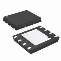
IC FLASH 4MBIT 33MHZ 8QFN
Manufacturer
Atmel
Datasheet
1.AT26F004-MU.pdf
(38 pages)
Specifications of AT26F004-MU
Format - Memory
FLASH
Memory Type
DataFLASH
Memory Size
4M (2048 pages x 256 bytes)
Speed
33MHz
Interface
SPI, 3-Wire Serial
Voltage - Supply
2.7 V ~ 3.6 V
Operating Temperature
-40°C ~ 85°C
Package / Case
8-VFQFN, 8-VFQFPN
Lead Free Status / RoHS Status
Lead free / RoHS Compliant
Available stocks
Company
Part Number
Manufacturer
Quantity
Price

Part Number:
AT26F004-MU
Manufacturer:
ATMEL/爱特梅尔
Quantity:
20 000


9. Protection Commands and Features
9.1
3588D–DFLASH–10/08
Write Enable
The Write Enable command is used to set the Write Enable Latch (WEL) bit in the Status Regis-
ter to a logical “1” state. The WEL bit must be set before a program, erase, Protect Sector,
Unprotect Sector, or Write Status Register command can be executed. This makes the issuance
of these commands a two step process, thereby reducing the chances of a command being
accidentally or erroneously executed. If the WEL bit in the Status Register is not set prior to the
issuance of one of these commands, then the command will not be executed.
To issue the Write Enable command, the CS pin must first be asserted and the opcode of 06h
must be clocked into the device. No address bytes need to be clocked into the device, and any
data clocked in after the opcode will be ignored. When the CS pin is deasserted, the WEL bit in
the Status Register will be set to a logical “1”. The complete opcode must be clocked into the
device before the CS pin is deasserted; otherwise, the device will abort the operation and the
state of the WEL bit will not change.
Figure 9-1.
Write Enable
SCK
SO
CS
SI
HIGH-IMPEDANCE
MSB
0
0
0
1
0
2
OPCODE
0
3
0
4
1
5
1
6
0
7
AT26F004
13
Related parts for AT26F004-MU
Image
Part Number
Description
Manufacturer
Datasheet
Request
R

Part Number:
Description:
DEV KIT FOR AVR/AVR32
Manufacturer:
Atmel
Datasheet:

Part Number:
Description:
INTERVAL AND WIPE/WASH WIPER CONTROL IC WITH DELAY
Manufacturer:
ATMEL Corporation
Datasheet:
Part Number:
Description:
Low-Voltage Voice-Switched IC for Hands-Free Operation
Manufacturer:
ATMEL Corporation
Datasheet:
Part Number:
Description:
MONOLITHIC INTEGRATED FEATUREPHONE CIRCUIT
Manufacturer:
ATMEL Corporation
Datasheet:
Part Number:
Description:
AM-FM Receiver IC U4255BM-M
Manufacturer:
ATMEL Corporation
Datasheet:
Part Number:
Description:
Monolithic Integrated Feature Phone Circuit
Manufacturer:
ATMEL Corporation
Datasheet:
Part Number:
Description:
Multistandard Video-IF and Quasi Parallel Sound Processing
Manufacturer:
ATMEL Corporation
Datasheet:
Part Number:
Description:
High-performance EE PLD
Manufacturer:
ATMEL Corporation
Datasheet:
Part Number:
Description:
8-bit Flash Microcontroller
Manufacturer:
ATMEL Corporation
Datasheet:
Part Number:
Description:
2-Wire Serial EEPROM
Manufacturer:
ATMEL Corporation
Datasheet: