AT26F004-MU Atmel, AT26F004-MU Datasheet - Page 22
AT26F004-MU
Manufacturer Part Number
AT26F004-MU
Description
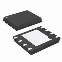
IC FLASH 4MBIT 33MHZ 8QFN
Manufacturer
Atmel
Datasheet
1.AT26F004-MU.pdf
(38 pages)
Specifications of AT26F004-MU
Format - Memory
FLASH
Memory Type
DataFLASH
Memory Size
4M (2048 pages x 256 bytes)
Speed
33MHz
Interface
SPI, 3-Wire Serial
Voltage - Supply
2.7 V ~ 3.6 V
Operating Temperature
-40°C ~ 85°C
Package / Case
8-VFQFN, 8-VFQFPN
Lead Free Status / RoHS Status
Lead free / RoHS Compliant
Available stocks
Company
Part Number
Manufacturer
Quantity
Price

Part Number:
AT26F004-MU
Manufacturer:
ATMEL/爱特梅尔
Quantity:
20 000


10.2
Write Status Register
The Write Status Register command is used to modify the SPRL bit of the Status Register.
Before the Write Status Register command can be issued, the Write Enable command must
have been previously issued to set the WEL bit in the Status Register to a logical “1”.
To issue the Write Status Register command, the CS pin must first be asserted and the opcode
of 01h must be clocked into the device. After the opcode has been clocked in, one byte of data
comprised of the SPRL bit value and seven don't care bits must be clocked in. Any additional
data bytes that are sent to the device will be ignored. When the CS pin is deasserted, the SPRL
bit in the Status Register will be modified, and the WEL bit in the Status Register will be reset
back to a logical “0”. The complete one byte of data must be clocked into the device before the
CS# pin is deasserted; otherwise, the device will abort the operation, the state of the SPRL bit
will not change, and the WEL bit in the Status Register will be reset back to the logical “0” state.
If the WP pin is asserted, then the SPRL bit can only be set to a logical “1”. If an attempt is made
to reset the SPRL bit to a logical “0” while the WP pin is asserted, then the Write Status Register
command will be ignored, and the WEL bit in the Status Register will be reset back to the logical
“0” state. In order to reset the SPRL bit to a logical “0”, the WP pin must be deasserted.
Figure 10-2. Write Status Register
CS
0
1
2
3
4
5
6
7
8
9
10 11
12
13
14 15
SCK
OPCODE
STATUS REGISTER IN
SI
0
0
0
0
0
0
0
1
D
X
X
X
X
X
X
X
MSB
MSB
HIGH-IMPEDANCE
SO
AT26F004
22
3588D–DFLASH–10/08
Related parts for AT26F004-MU
Image
Part Number
Description
Manufacturer
Datasheet
Request
R

Part Number:
Description:
DEV KIT FOR AVR/AVR32
Manufacturer:
Atmel
Datasheet:

Part Number:
Description:
INTERVAL AND WIPE/WASH WIPER CONTROL IC WITH DELAY
Manufacturer:
ATMEL Corporation
Datasheet:
Part Number:
Description:
Low-Voltage Voice-Switched IC for Hands-Free Operation
Manufacturer:
ATMEL Corporation
Datasheet:
Part Number:
Description:
MONOLITHIC INTEGRATED FEATUREPHONE CIRCUIT
Manufacturer:
ATMEL Corporation
Datasheet:
Part Number:
Description:
AM-FM Receiver IC U4255BM-M
Manufacturer:
ATMEL Corporation
Datasheet:
Part Number:
Description:
Monolithic Integrated Feature Phone Circuit
Manufacturer:
ATMEL Corporation
Datasheet:
Part Number:
Description:
Multistandard Video-IF and Quasi Parallel Sound Processing
Manufacturer:
ATMEL Corporation
Datasheet:
Part Number:
Description:
High-performance EE PLD
Manufacturer:
ATMEL Corporation
Datasheet:
Part Number:
Description:
8-bit Flash Microcontroller
Manufacturer:
ATMEL Corporation
Datasheet:
Part Number:
Description:
2-Wire Serial EEPROM
Manufacturer:
ATMEL Corporation
Datasheet: