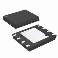
AT26F004-MU Atmel, AT26F004-MU Datasheet - Page 14

AT26F004-MU
Manufacturer Part Number
AT26F004-MU
Description
IC FLASH 4MBIT 33MHZ 8QFN
Manufacturer
Atmel
Datasheet
1.AT26F004-MU.pdf
(38 pages)
Specifications of AT26F004-MU
Format - Memory
FLASH
Memory Type
DataFLASH
Memory Size
4M (2048 pages x 256 bytes)
Speed
33MHz
Interface
SPI, 3-Wire Serial
Voltage - Supply
2.7 V ~ 3.6 V
Operating Temperature
-40°C ~ 85°C
Package / Case
8-VFQFN, 8-VFQFPN
Lead Free Status / RoHS Status
Lead free / RoHS Compliant
Available stocks
Company
Part Number
Manufacturer
Quantity
Price
Part Number:
AT26F004-MU
Manufacturer:
ATMEL/爱特梅尔
Quantity:
20 000
9.2
14
Write Disable
AT26F004
The Write Disable command is used to reset the Write Enable Latch (WEL) bit in the Status Reg-
ister to the logical “0” state. With the WEL bit reset, all program, erase, Protect Sector, Unprotect
Sector, and Write Status Register commands will not be executed. The Write Disable command
is also used to exit the Sequential Program mode. Other conditions can also cause the WEL bit
to be reset; for more details, refer to the
To issue the Write Disable command, the CS pin must first be asserted and the opcode of 04h
must be clocked into the device. No address bytes need to be clocked into the device, and any
data clocked in after the opcode will be ignored. When the CS pin is deasserted, the WEL bit in
the Status Register will be reset to a logical “0”. The complete opcode must be clocked into the
device before the CS pin is deasserted; otherwise, the device will abort the operation and the
state of the WEL bit will not change.
Figure 9-2.
Write Disable
SCK
SO
CS
SI
“WEL Bit” on page
HIGH-IMPEDANCE
MSB
0
0
0
1
0
2
OPCODE
0
3
0
4
1
5
0
6
0
20.
7
3588D–DFLASH–10/08


