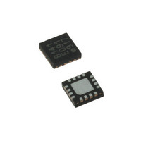
LDS8141-002-T2 IXYS, LDS8141-002-T2 Datasheet - Page 11

LDS8141-002-T2
Manufacturer Part Number
LDS8141-002-T2
Description
IC LED DRIVER WHIT BCKLGT 16WQFN
Manufacturer
IXYS
Series
LED-Sense™, Power-Lite™r
Type
Backlight, White LED (I²C Interface)r
Datasheet
1.LDS8141-002-T2.pdf
(22 pages)
Specifications of LDS8141-002-T2
Topology
High Side, Linear (LDO), PWM
Number Of Outputs
4
Internal Driver
Yes
Type - Primary
Backlight
Type - Secondary
White LED
Frequency
1.2MHz
Voltage - Supply
2.5 V ~ 5.5 V
Mounting Type
Surface Mount
Package / Case
16-WQFN, 16-miniQFN
Operating Temperature
-40°C ~ 85°C
Current - Output / Channel
32mA
Internal Switch(s)
Yes
Efficiency
80%
Lead Free Status / RoHS Status
Lead free / RoHS Compliant
Voltage - Output
-
Lead Free Status / Rohs Status
Details
Other names
LDS8141-002-T2-2
LDS8161/41
BLOCK DIAGRAM
BASIC OPERATION
The LDS8161 / 41 may operate in following modes:
NORMAL OPERATION MODE
At power-up, V
5.5 V (max). If V
logic LOW at least until V
When EN is taken HIGH, a soft-start power-up
sequence begins and performs an internal circuits
reset that requires less than 100 µs.
© 2009 IXYS Corp.
Characteristics subject to change without notice
a) Normal Operation Mode
b) Normal Standby Mode
c) Programming Modes
d) Shutdown Mode
SDA
SAD
GND
SCL
IN
should be in the range from 2.5 V to
32
IN
OTP
Driver
OTP
Trim
is slow rising, EN pin should be
Gnd
diagnostics
Soft Start control
LED Calibration
Top Level Control
Digital Temperature
Sensor / Abritrator
Vin to 1.8V LDO
for digital core
I2C Interface
IN
Shorted LED
Open LED
De-Rating
Temp to PWM
reaches a 2.5 V level.
De-Rating
adjust LUTs
Temp
LUT
Temp
Temp
Table
1.8V
Figure 2: LDS8161/41 Functional Block Diagram
Vin
1 0 uA
10
To top control
1.2V
1.2V
Si Iforce
Reference
10 bit SAR
Bandgap
Voltage
8 bit to 12 bit (log) PWM
1.2V
ADC
Si PNP
temp diode
Start Up
POR
VIN
2 uA
Pre-Scale
8x, 1x, or 1/4x
Generator
to top control & dig processing
EN
PWM
1 mA
11
OverTemp
LED Iforce
Reference
Calibrated
ADC bias
currents
Currents
Oscillator & Clock Generator
0.2 mA
An initialization sequence then begins, taking less
than 10 ms. This sequence determines the user-
selected
programmed settings, and conducts diagnostics for
open/shorted LEDs.
At this point, the I
communication and the LDS8161/41 may be user-
programmed. Upon programming completion for all
required initial parameters and features’ settings, a
calibration command is given by setting bit 4 of the
Control Register (1Fh)
calibration sequence of the LDS8161/41 LED-
Sense
simultaneous with a gradual ramp-up of LED PWM
and current levels to the user programmed values.
This initialization is completed in less than 250 ms in
and
to PWM
TM
~ 1.2 MHz
Vin to
al l
Drivers
temperature de-rating circuits and occurs
I
2
C
slave
All Drivers 0 to 31.875 mA
PWM
PWM
PWM
PWM
PWM
PWM
2
Vin
C interface is ready for
Doc. No. 8141/61_DS, Rev. N1.0
address,
HIGH. This starts the
loads
LEDA1
LEDA2
LEDB1
LEDB2
LEDC1
(8161)
LEDC2
(8161)
factory


