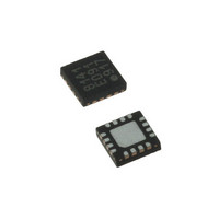
LDS8141-002-T2 IXYS, LDS8141-002-T2 Datasheet - Page 4

LDS8141-002-T2
Manufacturer Part Number
LDS8141-002-T2
Description
IC LED DRIVER WHIT BCKLGT 16WQFN
Manufacturer
IXYS
Series
LED-Sense™, Power-Lite™r
Type
Backlight, White LED (I²C Interface)r
Datasheet
1.LDS8141-002-T2.pdf
(22 pages)
Specifications of LDS8141-002-T2
Topology
High Side, Linear (LDO), PWM
Number Of Outputs
4
Internal Driver
Yes
Type - Primary
Backlight
Type - Secondary
White LED
Frequency
1.2MHz
Voltage - Supply
2.5 V ~ 5.5 V
Mounting Type
Surface Mount
Package / Case
16-WQFN, 16-miniQFN
Operating Temperature
-40°C ~ 85°C
Current - Output / Channel
32mA
Internal Switch(s)
Yes
Efficiency
80%
Lead Free Status / RoHS Status
Lead free / RoHS Compliant
Voltage - Output
-
Lead Free Status / Rohs Status
Details
Other names
LDS8141-002-T2-2
LDS8161/41
Option 1: Standard protocol sequential read:
where Reg. m is the last addressed in the write operation register
Option 2: Random access:
Option 3: Random access with combined (extended) protocol:
Option 1: Standard protocol sequencial write:
© 2009 IXYS Corp.
Characteristics subject to change without notice
I
Over recommended operating conditions unless otherwise specified for 2.7 VIN 5.5V, over full ambient temperature range -40 to +85ºC.
2
C CHARACTERISTICS
Symbol
t
t
t
t
t
S
S
S
S
HD:STA
SU:STA
HD:DAT
SU:DAT
SU:STO
t
t
f
t
LOW
HIGH
READ OPERATION:
WRITE OPERATION:
BUF
t
t
SCL
t
t
DH
AA
R
F
Slave Address
Slave Address
Slave Address
Slave Address
Parameter
SCL Clock Frequency
Hold Time (repeated) START condition
LOW period of the SCL clock
HIGH period of the SCL clock
Set-up Time for a repeated START condition
Data In Hold Time
Data In Set-up Time
Rise Time of both SDAT and SCLK signals
Fall Time of both SDAT and SCLK signals
Set-up Time for STOP condition
Bus Free Time between a STOP and START condition
SCLK Low to SDAT Data Out and ACK Out
Data Out Hold Time
W
W
R
R
A
A
A
From reg. m, where Reg. m is the last addressed in the write operation register
A
Register Address m
Register Address m
From: Reg. m
Data m
Data 0
Figure 1: I
A*
A
2
Reg. m+1
P
C Bus Timing Diagram
Data 1
A
4
To: Reg. m
A
Data 0
A
Sr
Reg. m+2
Data 2
Slave Address
A
Reg. m+1
Data 1
Min
100
300
0.6
1.3
0.6
0.6
0.6
1.3
A
0
0
Reg. m+n,
R
Data n
Reg. m+2
Data 2
Doc. No. 8141/61_DS, Rev. N1.0
Max
A
400
300
300
0.9
0.9
A*
Reg. m+k
Data m
P
Data k
Unit
kHz
µs
µs
µs
µs
ns
ns
ns
ns
µs
µs
µs
ns
A*
A*
P
P


