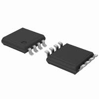
PCA9632DP1,118 NXP Semiconductors, PCA9632DP1,118 Datasheet - Page 12

PCA9632DP1,118
Manufacturer Part Number
PCA9632DP1,118
Description
IC LED DRIVER RGBA 8-TSSOP
Manufacturer
NXP Semiconductors
Type
RGBA LED Driverr
Datasheet
1.PCA9632TK118.pdf
(38 pages)
Specifications of PCA9632DP1,118
Package / Case
8-TSSOP
Topology
Open Drain, PWM
Number Of Outputs
4
Internal Driver
Yes
Type - Primary
Backlight, LED Blinker
Type - Secondary
RGBA
Frequency
1MHz
Voltage - Supply
2.3 V ~ 5.5 V
Voltage - Output
5.5V
Mounting Type
Surface Mount
Operating Temperature
-40°C ~ 85°C
Current - Output / Channel
25mA
Internal Switch(s)
Yes
Number Of Segments
4
Low Level Output Current
100000 uA
Operating Supply Voltage
2.3 V to 5.5 V
Maximum Supply Current
150 uA
Maximum Power Dissipation
400 mW
Maximum Operating Temperature
+ 85 C
Mounting Style
SMD/SMT
Minimum Operating Temperature
- 40 C
Lead Free Status / RoHS Status
Lead free / RoHS Compliant
Efficiency
-
Lead Free Status / Rohs Status
Lead free / RoHS Compliant
Other names
935284899118
PCA9632DP1-T
PCA9632DP1-T
PCA9632DP1-T
PCA9632DP1-T
Available stocks
Company
Part Number
Manufacturer
Quantity
Price
Part Number:
PCA9632DP1,118
Manufacturer:
NXP/恩智浦
Quantity:
20 000
NXP Semiconductors
PCA9632_3
Product data sheet
7.3.3 PWM registers 0 to 3, PWMx — Individual brightness control registers
Table 8.
Legend: * default value.
While operating in Individual brightness mode (LDRx = 10), a 1.5625 kHz fixed frequency
signal is used for each output. Duty cycle is controlled through 256 linear steps from 00h
(0 % duty cycle = LED output off) to FFh (99.6 % duty cycle = LED output at maximum
brightness). In this mode, all the 8 bits are used.
E.g., if IDCx[7:0] = 1111 1111, then duty cycle = 255 / 256 = 99.6 %.
While operating in group dimming mode, a 6.25 kHz fixed frequency signal is used for
each output. Duty cycle is controlled through 64 linear steps from 00h (0 % duty cycle =
LED output off) to 3Fh (98.4 % duty cycle = LED output at maximum brightness). In this
mode only the 6 MSBs are used (IDCx[7:2]). The 2 LSBs IDCx[1:0] are ignored.
Applicable to LED outputs programmed with LDRx = 11 (LEDOUT register).
E.g., if IDCx[7:2] = 111111, then duty cycle = 1111 1100 / 256 = 252 / 256 = 98.4 %.
While operating in blink mode, a 1.5625 kHz fixed frequency signal is used for each
output. Duty cycle is controlled through 256 linear steps from 00h (0 % duty cycle = LED
output off) to FFh (99.6 % duty cycle = LED output at maximum brightness). In this mode,
all the 8 bits are used.
E.g., if IDCx[7:0] = 1111 1111, then duty cycle = 255 / 256 = 99.6 %.
Applicable to LED outputs programmed with LDRx = 11 (LEDOUT register).
duty cycle
duty cycle
duty cycle
Address
02h
03h
04h
05h
Register
PWM0
PWM1
PWM2
PWM3
PWM0 to PWM3 - PWM registers 0 to 3 (address 02h to 05h) bit description
=
=
=
-------------------------- -
-----------------------------------
-------------------------- -
IDCx 7:0
IDCx 7:2 ,00
IDCx 7:0
256
256
256
Bit
7:0
7:0
7:0
7:0
Rev. 03 — 15 July 2008
Symbol
IDC0[7:0]
IDC1[7:0]
IDC2[7:0]
IDC3[7:0]
Access Value
R/W
R/W
R/W
R/W
4-bit Fm+ I
0000 0000* PWM0 Individual Duty Cycle
0000 0000* PWM1 Individual Duty Cycle
0000 0000* PWM2 Individual Duty Cycle
0000 0000* PWM3 Individual Duty Cycle
2
C-bus low power LED driver
Description
PCA9632
© NXP B.V. 2008. All rights reserved.
12 of 38
(1)
(2)
(3)


