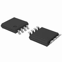
PCA9632DP1,118 NXP Semiconductors, PCA9632DP1,118 Datasheet - Page 27

PCA9632DP1,118
Manufacturer Part Number
PCA9632DP1,118
Description
IC LED DRIVER RGBA 8-TSSOP
Manufacturer
NXP Semiconductors
Type
RGBA LED Driverr
Datasheet
1.PCA9632TK118.pdf
(38 pages)
Specifications of PCA9632DP1,118
Package / Case
8-TSSOP
Topology
Open Drain, PWM
Number Of Outputs
4
Internal Driver
Yes
Type - Primary
Backlight, LED Blinker
Type - Secondary
RGBA
Frequency
1MHz
Voltage - Supply
2.3 V ~ 5.5 V
Voltage - Output
5.5V
Mounting Type
Surface Mount
Operating Temperature
-40°C ~ 85°C
Current - Output / Channel
25mA
Internal Switch(s)
Yes
Number Of Segments
4
Low Level Output Current
100000 uA
Operating Supply Voltage
2.3 V to 5.5 V
Maximum Supply Current
150 uA
Maximum Power Dissipation
400 mW
Maximum Operating Temperature
+ 85 C
Mounting Style
SMD/SMT
Minimum Operating Temperature
- 40 C
Lead Free Status / RoHS Status
Lead free / RoHS Compliant
Efficiency
-
Lead Free Status / Rohs Status
Lead free / RoHS Compliant
Other names
935284899118
PCA9632DP1-T
PCA9632DP1-T
PCA9632DP1-T
PCA9632DP1-T
Available stocks
Company
Part Number
Manufacturer
Quantity
Price
Part Number:
PCA9632DP1,118
Manufacturer:
NXP/恩智浦
Quantity:
20 000
NXP Semiconductors
13. Dynamic characteristics
Table 19.
[1]
[2]
[3]
[4]
[5]
[6]
[7]
PCA9632_3
Product data sheet
Symbol Parameter
f
t
t
t
t
t
t
t
t
t
t
t
t
t
SCL
BUF
HD;STA
SU;STA
SU;STO
HD;DAT
VD;ACK
VD;DAT
SU;DAT
LOW
HIGH
f
r
SP
Minimum SCL clock frequency is limited by the bus time-out feature, which resets the serial bus interface if either SDA or SCL is held
LOW for a minimum of 25 ms. Disable bus time-out feature for DC operation.
t
t
A master device must internally provide a hold time of at least 300 ns for the SDA signal (refer to
to bridge the undefined region of SCL’s falling edge.
The maximum t
250 ns. This allows series protection resistors to be connected between the SDA and the SCL pins and the SDA/SCL bus lines without
exceeding the maximum specified t
C
Input filters on the SDA and SCL inputs suppress noise spikes less than 50 ns.
VD;ACK
VD;DAT
b
= total capacitance of one bus line in pF.
SCL clock frequency
bus free time between a
STOP and START condition
hold time (repeated) START
condition
set-up time for a repeated
START condition
set-up time for STOP
condition
data hold time
data valid acknowledge time
data valid time
data set-up time
LOW period of the SCL
clock
HIGH period of the SCL
clock
fall time of both SDA and
SCL signals
rise time of both SDA and
SCL signals
pulse width of spikes that
must be suppressed by the
input filter
= minimum time for SDA data out to be valid following SCL LOW.
= time for Acknowledgement signal from SCL LOW to SDA (out) LOW.
Dynamic characteristics
f
for the SDA and SCL bus lines is specified at 300 ns. The maximum fall time (t
f
.
Conditions
Rev. 03 — 15 July 2008
[4][5]
[1]
[2]
[3]
[7]
Standard- mode
Min
250
4.7
4.0
4.7
4.0
0.3
0.3
4.7
4.0
0
0
-
-
-
I
2
C-bus
1000
Max
3.45
3.45
100
300
50
-
-
-
-
-
-
-
-
4-bit Fm+ I
20 + 0.1C
20 + 0.1C
Fast-mode
Min
100
1.3
0.6
0.6
0.6
0.1
0.1
1.3
0.6
0
0
I
-
2
C-bus
f
) for the SDA output stage is specified at
Table
b
b
2
[6]
[6]
C-bus low power LED driver
Max
18, V
400
300
300
0.9
0.9
50
-
-
-
-
-
-
-
-
IL
of the SCL signal) in order
Plus I
0.26
0.26
0.26
0.05
0.05
0.26
Min
PCA9632
0.5
0.5
50
Fast-mode
© NXP B.V. 2008. All rights reserved.
0
0
-
-
-
2
C-bus
1000
Max
0.45
0.45
120
120
50
-
-
-
-
-
-
-
-
27 of 38
Unit
kHz
ns
ns
ns
ns
ns
s
s
s
s
s
s
s
s


