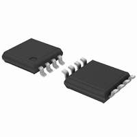
PCA9632DP1,118 NXP Semiconductors, PCA9632DP1,118 Datasheet - Page 24

PCA9632DP1,118
Manufacturer Part Number
PCA9632DP1,118
Description
IC LED DRIVER RGBA 8-TSSOP
Manufacturer
NXP Semiconductors
Type
RGBA LED Driverr
Datasheet
1.PCA9632TK118.pdf
(38 pages)
Specifications of PCA9632DP1,118
Package / Case
8-TSSOP
Topology
Open Drain, PWM
Number Of Outputs
4
Internal Driver
Yes
Type - Primary
Backlight, LED Blinker
Type - Secondary
RGBA
Frequency
1MHz
Voltage - Supply
2.3 V ~ 5.5 V
Voltage - Output
5.5V
Mounting Type
Surface Mount
Operating Temperature
-40°C ~ 85°C
Current - Output / Channel
25mA
Internal Switch(s)
Yes
Number Of Segments
4
Low Level Output Current
100000 uA
Operating Supply Voltage
2.3 V to 5.5 V
Maximum Supply Current
150 uA
Maximum Power Dissipation
400 mW
Maximum Operating Temperature
+ 85 C
Mounting Style
SMD/SMT
Minimum Operating Temperature
- 40 C
Lead Free Status / RoHS Status
Lead free / RoHS Compliant
Efficiency
-
Lead Free Status / Rohs Status
Lead free / RoHS Compliant
Other names
935284899118
PCA9632DP1-T
PCA9632DP1-T
PCA9632DP1-T
PCA9632DP1-T
Available stocks
Company
Part Number
Manufacturer
Quantity
Price
Part Number:
PCA9632DP1,118
Manufacturer:
NXP/恩智浦
Quantity:
20 000
NXP Semiconductors
10. Application design-in information
PCA9632_3
Product data sheet
Question 1: What kind of edge rate control is there on the outputs?
Question 2: Is ground bounce possible?
Question 3: Can I really sink 400 mA through the single ground pin on the package and
will this cause any ground bounce problem due to the PWM of the LEDs?
Question 4: I can’t turn the LEDs on or off, but their registers are set properly. Why?
Fig 21. Typical application
•
•
•
•
I
The typical edge rates depend on the output configuration, supply voltage, and the
applied load. The outputs can be configured as either open-drain NMOS or totem pole
outputs. If the customer is using the part to directly drive LEDs, they should be using it
in an open-drain NMOS, if they are concerned about the maximum I
bounce. The edge rate control was designed primarily to slow down the turn-on of the
output device; it turns off rather quickly (~ 1.5 ns). In simulation, the typical turn-on
time for the open-drain NMOS was ~ 14 ns (V
Ground bounce is a possibility, especially if all 16 outputs transition at full current
(25 mA each). There is a fair amount of decoupling capacitance on chip (~ 50 pF),
which is intended to suppress some of the ground bounce. The customer will need to
determine if additional decoupling capacitance externally placed as close as
physically possible to the device is required.
Yes, you can sink 400 mA through a single ground pin on the package. Although the
package only has one ground pin, there are two ground pads on the die itself
connected to this one pin. Although some ground bounce is likely, it will not disrupt the
operation of the part and would be reduced by the external decoupling capacitance.
Check the Mode register 1 bit 4 (MODE1[4]) SLEEP setting. The value needs to be a
logic 0 so that the OSC is turned on. If the OSC is turned off, the LEDs cannot be
turned on or off and also can’t be dimmed or blinked.
2
C-BUS/SMBus
MASTER
V
DD
I
All of the 4 LED outputs configurable as either open-drain or totem pole. Mixing of configurations is
not possible.
2
= 2.5 V, 3.3 V or 5.0 V
C-bus address = 1100 001X.
SDA
SCL
10 k
Rev. 03 — 15 July 2008
10 k
SDA
SCL
A0
A1
V
SS
PCA9632
V
DD
4-bit Fm+ I
002aad049
LED0
LED1
LED2
LED3
DD
= 3.6 V; C
2
5 V
C-bus low power LED driver
L
= 50 pF; R
PCA9632
© NXP B.V. 2008. All rights reserved.
SS
and ground
PU
= 500 ).
12 V
24 of 38


