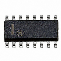
NCP1650DR2 ON Semiconductor, NCP1650DR2 Datasheet - Page 15

NCP1650DR2
Manufacturer Part Number
NCP1650DR2
Description
IC CTRLR PWR FACTOR PWM 16SOIC
Manufacturer
ON Semiconductor
Datasheet
1.NCP1650DR2G.pdf
(31 pages)
Specifications of NCP1650DR2
Mode
Continuous Conduction (CCM), Discontinuous Conduction (DCM)
Frequency - Switching
100kHz
Voltage - Supply
10 V ~ 20 V
Operating Temperature
-40°C ~ 125°C
Mounting Type
Surface Mount
Package / Case
16-SOIC (3.9mm Width)
Switching Frequency
25 KHz to 250 KHz
Maximum Operating Temperature
+ 125 C
Mounting Style
SMD/SMT
Minimum Operating Temperature
- 40 C
Lead Free Status / RoHS Status
Contains lead / RoHS non-compliant
Current - Startup
-
Lead Free Status / Rohs Status
Lead free / RoHS Compliant
Other names
NCP1650DR2OSTR
Available stocks
Company
Part Number
Manufacturer
Quantity
Price
Part Number:
NCP1650DR2G
Manufacturer:
ON/安森美
Quantity:
20 000
into a high quality sine wave is the operation of the AC error
amplifier. The inputs of an operational amplifier operating
in its linear range, must be equal.
differences between the inverting and non- -inverting inputs,
but for the purpose of this analysis they can be considered to
be equal.
multiplier is fed into the non- -inverting input of the AC error
amplifier. The inverting input to the AC error amplifier
receives a signal that is comprised of the input fullwave
rectified sinewave (which is not modified by the reference
multiplier), and summed with the filtered input current.
Since the two inputs to this amplifier will be at the same
potential, the complex signal at the inverting input will have
the same wave shape as the AC reference signal. The AC
reference signal (V
the AC input signal (V
sinewave, therefore, the AC current signal (I
a fullwave rectified sinewave. This relationship gives the
formula:
value will not follow the low frequency fullwave rectified
sinewave exactly, however, the output of the AC error
amplifier has a low frequency pole that allows the average
value of the .75 V
error amplifier is a transconductance amplifier, it is followed
by an inverting unity gain buffer stage with a low impedance
AC INPUT
The key to understanding how the input current is shaped
There are several secondary effects, that create small
The fullwave rectified sinewave output of the reference
The I
COMP
LOOP
FB/SD
in
signal has a wide bandwidth, and its instantaneous
V ref = .75 · V line + (k · I in )
AVERAGE CURRENT
4 V
COMPENSATION
line
+
--
ref
REFERENCE
.75
MULTIPLIER
) is a fullwave rectified sinewave, and
+ (k x I
--
+
line
V
VOLTAGE
line
Figure 32. Simplified Block Diagram of Basic PFC Control Circuit
ERROR
) is also a fullwave rectified
in
AMP
) to follow V
V
error(dc)
V
ref
AC ERROR
+
--
ref
in
AMP
. Since the AC
V
), must also be
error(ac)
4 V
http://onsemi.com
REFERENCE
REF FILTER
V--I
BUFFER
+
--
AC
PWM
15
V
error(ac)
output so that the signal can be summed with the
instantaneous input switching current (I
buffer is still V
V
error(ac)
V
line
k I
PWM
Logic
AC Input
V
V
error(ac)
error(ac)
+ k I
Figure 33. Typical Signals for PFC Circuit
in
k I
V
V
line
ref
in
in
AMPLIFIER
CURRENT
error
SENSE
DRIVER
ac
.
V
error(ac)
DRIVE
1
I
S--
V
ref
in
+Bus
--Bus
). The output of the
OSC
4 V ref
GND
4 V ref
GND
R
R
ac1
ac2


