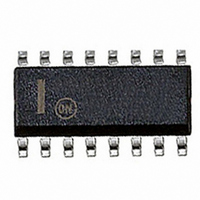
NCP1650DR2 ON Semiconductor, NCP1650DR2 Datasheet - Page 27

NCP1650DR2
Manufacturer Part Number
NCP1650DR2
Description
IC CTRLR PWR FACTOR PWM 16SOIC
Manufacturer
ON Semiconductor
Datasheet
1.NCP1650DR2G.pdf
(31 pages)
Specifications of NCP1650DR2
Mode
Continuous Conduction (CCM), Discontinuous Conduction (DCM)
Frequency - Switching
100kHz
Voltage - Supply
10 V ~ 20 V
Operating Temperature
-40°C ~ 125°C
Mounting Type
Surface Mount
Package / Case
16-SOIC (3.9mm Width)
Switching Frequency
25 KHz to 250 KHz
Maximum Operating Temperature
+ 125 C
Mounting Style
SMD/SMT
Minimum Operating Temperature
- 40 C
Lead Free Status / RoHS Status
Contains lead / RoHS non-compliant
Current - Startup
-
Lead Free Status / Rohs Status
Lead free / RoHS Compliant
Other names
NCP1650DR2OSTR
Available stocks
Company
Part Number
Manufacturer
Quantity
Price
Part Number:
NCP1650DR2G
Manufacturer:
ON/安森美
Quantity:
20 000
Voltage Loop
Block Diagram
into four sections. These are the voltage divider, voltage error
amplifier, reference signal and modulator and output stage.
simplified based on the assumption that that poles and zeros
in the current feedback loop are considerably greater than
the bandwidth of the overall loop. This should be a good
assumption, because a bandwidth in the kilohertz is
necessary for a good current waveform, and the voltage error
amplifier needs to have a bandwidth of less than the lowest
line frequency that will be used.
pole that varies with the load. The pole on the voltage error
amplifier will be determined by this analysis.
Voltage Divider
reduces the output voltage to the 4.0 volt level required by
the internal reference on the voltage error amplifier.
Voltage Error Amplifier
equations. When this amplifier is compensated with a
pole- -zero pair, there will be a unity gain pole which will be
cancelled by the zero at frequency f
bode plot would be:
V o
V
V′
DIVIDER
The block diagram for the voltage loop has been broken down
The modulator and output stage circuitry is greatly
There are two poles in this circuit. The output filter has a
The voltage divider is a simple resistive divider that
The voltage error amplifier is constrained by the three
R
FB/SD
R
=
dc1
dc2
R dc1 + R dc2
6
R dc2
4 V
+
--
LOOP COMP
ERROR
(High Frequency Gain, Past Zero)
AMP
V
e/a
f unity =
f z =
A v = G m R 7
ERROR AMP
R
7
C
7
2 π C 7 R 7
7
ORing NET
--0.32 mA/V
2 π C 7
1
G m
R
ac2
Z
. The corresponding
Figure 41. Voltage Loop Model
REFERENCE
REFERENCE SIGNAL
MULTIPLIER
V e∕a
V ac =
V ref
V
Loop Compensation
ac
http://onsemi.com
= --2 V ac
R ac1 + R ac2
25 k
V line R ac2
V
ref
27
ERROR
AMP
R
AC
Reference Signal
network, which has a negative gain, and is then used as an
input to the reference multiplier. The gain of this block is
dependent on the AC input voltage, because of the multiplier
which requires two inputs for one output.
Modulator and Output Stage
reference multiplier and forces the current to follow the
shape and amplitude of the reference signal. The current
shaping circuit is an internal loop within this section due to
the current sense amplifier. Based on the assumptions listed
ac1
+
--
--20
The output of the error amplifier is modified by the ORing
The AC error amplifier receives an input from the
20
0
4 V
I
C.S. Amp
avg
V
--
+
MODULATOR AND OUTPUT STAGE
line
Figure 42. Pole- -Zero Bode Plot
UNITY GAIN
PWM
10
R
10
ΔV ref
f p =
ΔV o
LOGIC
FREQUENCY
2 π R C
=
1
225k R S
R L R 10
OUT
16
12
I
S--
RECTIFIER
Q1
R
S
Av
C
V
R
o
L


