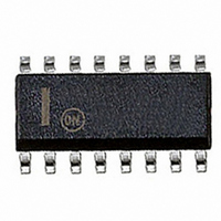
NCP1650DR2 ON Semiconductor, NCP1650DR2 Datasheet - Page 5

NCP1650DR2
Manufacturer Part Number
NCP1650DR2
Description
IC CTRLR PWR FACTOR PWM 16SOIC
Manufacturer
ON Semiconductor
Datasheet
1.NCP1650DR2G.pdf
(31 pages)
Specifications of NCP1650DR2
Mode
Continuous Conduction (CCM), Discontinuous Conduction (DCM)
Frequency - Switching
100kHz
Voltage - Supply
10 V ~ 20 V
Operating Temperature
-40°C ~ 125°C
Mounting Type
Surface Mount
Package / Case
16-SOIC (3.9mm Width)
Switching Frequency
25 KHz to 250 KHz
Maximum Operating Temperature
+ 125 C
Mounting Style
SMD/SMT
Minimum Operating Temperature
- 40 C
Lead Free Status / RoHS Status
Contains lead / RoHS non-compliant
Current - Startup
-
Lead Free Status / Rohs Status
Lead free / RoHS Compliant
Other names
NCP1650DR2OSTR
Available stocks
Company
Part Number
Manufacturer
Quantity
Price
Part Number:
NCP1650DR2G
Manufacturer:
ON/安森美
Quantity:
20 000
4. Verified by design.
ELECTRICAL CHARACTERISTICS
typical values. For min/max values T
MAXIMUM POWER MULTIPLIER
AC INPUT (Pin 5)
DRIVE OUTPUT
VOLTAGE REFERENCE
UNDERVOLTAGE LOCKOUT/SHUTDOWN
OVERVOLTAGE PROTECTION
TOTAL DEVICE
Multiplier Gain
R
Dynamic Input Voltage Range
Input Bias Current
Source Resistance (80 mA Load)
Sink Resistance (--80 mA Load)
Rise Time (C
Fall Time (C
Output Voltage in UVLO Condition
4.0 Volt Reference (Pin 6) (T
4.0 Volt Regulation (T
2.5 Volt Reference (P
Buffered Output (I
Load Regulation (Buffered Output, Io = 0 to 10 mA, V
UVLO Startup Threshold (V
UVLO Hysteresis (Shutdown Voltage = V
Shutdown Startup Threshold (Pin 6) (V
Shutdown Hysteresis (Pin 6)
Overvoltage Voltage Trip Point (V
Overvoltage Voltage Differential (V
Operational Bias Current (C
Bias Current in Undervoltage Mode
(Total bias current for both multipliers and current compensation amplifier)
9
Ac Input (p--input) (Note 4)
= 47 k, R
L
10
K =
L
= 1.0 nF, 20% to 80%)
= 1.0 nF, 20% to 80%)
= 15 k
(--V pin12 ) × V pin5
load
max
J
= 0 mA)
= --55C to 125C)
V pin9
, Pin 9)
CC
L(Driver)
J
= 25C)
Characteristic
Increasing)
pin6
OV
J
= 1.0 nF, 100 kHz)
is the applicable junction temperature.)
/V
≈
-- V
out
ref
4.0 × R 9
(continued) (Unless otherwise noted: V
SU
)
boost+
Increasing)
R 10
– V
)
H
)
CC
(T
J
http://onsemi.com
> 10 V)
= --40C to +125C)
(T
5
J
= 25C)
CC
DVref
I
Bshutdown
Symbol
Vref
R
V
Vref
V
I
V
R
I
= 14 volts, C
INbias
Vref
Vref
V
V
V
source
O(UV)
OVdiff
BIAS
V
V
max
sink
k
t
t
SU
SD
OV
r
f
OUT
H
H
2.5
OUT
T
106.5
12.1
3.94
3.92
2.40
6.24
0.50
0.10
11.8
Min
4.0
3.0
0.3
= 470 pF, C
10
0
--
--
--
--
--
--
--
--
12.8
12.8
3.75
0.01
4.00
4.00
2.50
6.50
10.5
0.85
0.18
Typ
108
8.0
8.0
1.0
4.0
0.5
4.0
0.6
50
50
50
2
= 0.1 mF, T
109.5
Max
13.3
13.3
4.06
4.08
2.60
6.76
1.00
0.7
0.3
5.0
1.0
15
15
10
40
11
--
--
--
--
--
J
= 25C for
1.0/V
Unit
mV
mV
V/V
mV
mA
mA
mA
ns
ns
Ω
Ω
V
V
V
V
V
V
V
V
V


