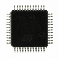
L6740LTR STMicroelectronics, L6740LTR Datasheet - Page 11

L6740LTR
Manufacturer Part Number
L6740LTR
Description
IC HYBRID CONTROLLERS 48TQFP
Manufacturer
STMicroelectronics
Datasheet
1.L6740LTR.pdf
(44 pages)
Specifications of L6740LTR
Applications
Hybrid Controllers
Voltage - Supply
9 V ~ 15 V
Current - Supply
20mA
Operating Temperature
0°C ~ 125°C
Mounting Type
Surface Mount
Package / Case
48-TQFP Exposed Pad, 48-eTQFP, 48-HTQFP, 48-VQFP
Number Of Outputs
2
Output Current
170 A
Input Voltage
13.2 V
Mounting Style
SMD/SMT
Maximum Operating Temperature
+ 125 C
Minimum Operating Temperature
0 C
Lead Free Status / RoHS Status
Lead free / RoHS Compliant
Voltage - Input
-
Lead Free Status / Rohs Status
Lead free / RoHS Compliant
Other names
497-6298-2
Available stocks
Company
Part Number
Manufacturer
Quantity
Price
Part Number:
L6740LTR
Manufacturer:
ST
Quantity:
20 000
L6740L
Table 2.
35,
31
32
33
34
36
37
39
40
Pin#
38
41
Pin description (continued)
NB_DROOP
PWRGOOD
SVC / VID3
SVD / VID2
NB_COMP
VID0, VID1
NB_VSEN
PWROK
NB_FB
Name
EN
NB output voltage monitor.
It manages OVP and UVP protections and PWRGOOD. Connect to the
positive side of the NB load to perform remote sensing. See
for proper layout of this connection.
A current proportional to the total current read by the NB section is
sourced through this pin according to the current reading gain (R
Short to NB_FB to implement Droop Function or connect to SGND
through a resistor and filter with 1nF capacitor to implement NB LOAD
Indicator. If not used, short to SGND.
NB error amplifier inverting input.
Connect with a resistor R
to NB_COMP. Offset current programmed by NB_OS is sunk through
this pin.
Error amplifier output.
Connect with an R
cannot be disabled by grounding this pin.
Voltage IDentification pins.
Internally pulled-low by 10 μA, they are used to program the output
voltage. VID1 is monitored on the EN pin rising-edge to define the
operative mode of the controller (SVI or PVI). When in SVI mode, VID0
is ignored. See
System-wide Power Good input (SVI mode).
Internally pulled-low by 10 μA. When low, the device will decode the two
SVI bits (SVC, SVD) to determine the Pre-PWROK Metal VID (default
condition when pin is floating).
When high, the device will actively run the SVI protocol.
Pre-PWROK Metal VID are latched after EN is asserted and re-used in
case of PWROK de-assertion. Latch is reset by VCC or EN cycle.
VR Enable. Internally pulled-up to 3.3 V by 10 μA.
Pull-low to disable the device. When set free, the device immediately
checks for the VID1 status to determine the SVI / PVI protocol to be
adopted and configures itself accordingly. See
Voltage IDentification pin - SVI clock pin.
Internally pulled-low by 10 μA, it is used to program the output voltage.
When in SVI-mode, it is considered as Serial-VID-data (input / open
drain output). See
Voltage IDentification pins - SVI data pin.
Internally pulled-low by 10 μA, it is used to program the output voltage.
When in SVI-mode, it is considered as Serial-VID-data (input / open
drain output). See
VCORE and NB Power Good.
It is an open-drain output set free after SS as long as both the voltage
planes are within specifications. Pull-up to 3.3V (typ) or lower, if not
used it can be left floating.
When in PVI mode, it monitors the CORE section only.
Section 5
F_NB
Section 5
Section 5
Pins description and connection diagrams
- C
FB_NB
for details.
F_NB
for details.
for details.
Function
to NB_VSEN and with an R
to NB_FB. The NB section or the device
Section 5
for details.
F_NB
Section 9
- C
ISEN
F_NB
11/44
).


