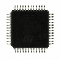
L6740LTR STMicroelectronics, L6740LTR Datasheet - Page 27

L6740LTR
Manufacturer Part Number
L6740LTR
Description
IC HYBRID CONTROLLERS 48TQFP
Manufacturer
STMicroelectronics
Datasheet
1.L6740LTR.pdf
(44 pages)
Specifications of L6740LTR
Applications
Hybrid Controllers
Voltage - Supply
9 V ~ 15 V
Current - Supply
20mA
Operating Temperature
0°C ~ 125°C
Mounting Type
Surface Mount
Package / Case
48-TQFP Exposed Pad, 48-eTQFP, 48-HTQFP, 48-VQFP
Number Of Outputs
2
Output Current
170 A
Input Voltage
13.2 V
Mounting Style
SMD/SMT
Maximum Operating Temperature
+ 125 C
Minimum Operating Temperature
0 C
Lead Free Status / RoHS Status
Lead free / RoHS Compliant
Voltage - Input
-
Lead Free Status / Rohs Status
Lead free / RoHS Compliant
Other names
497-6298-2
Available stocks
Company
Part Number
Manufacturer
Quantity
Price
Part Number:
L6740LTR
Manufacturer:
ST
Quantity:
20 000
L6740L
6.6
Caution:
Note:
6.7
NB section - load-line and load-indicator (optional)
This method introduces a dependence of the output voltage on the load current recovering
part of the drop due to the output capacitor ESR in the load transient. Introducing a depen-
dence of the output voltage on the load current, a static error, proportional to the output cur-
rent, causes the output voltage to vary according to the sensed current.
Figure 10
ing across the low-side MOSFET is read through R
tance gain and generates a current I
section that is then sourced by the NB_FB pin (I
program the desired load-line slope
The output characteristic vs. load current is then given by (Offset disabled):
Where R
The whole power supply can be then represented by a “real” voltage generator with an
equivalent output resistance R
R
Load-line (DROOP) implementation is optional, in case it is not desired, the resulting current
information may be employed for other purposes, such as load indicator (LI). In this case,
simply connect a resistor R
proportional to the delivered current according to the following relationship:
Split between R
where the Droop effect is minimum (i.e. < 50 mV over 100 A) to simplify the compensation
network design.
NB section - offset (optional)
The NB_OS pin allows programming a positive offset (V
voltage by connecting a resistor R
current is programmed by connecting the resistor R
current is mirrored and then properly sunk from the NB_FB pin as shown in
voltage is then programmed as follow:
Offset resistor can be designed by considering the following relationship (R
fixed by the droop effect):
V
R
V
V
OUT_NB
FB_NB
NB_DROOP
NB
FB_NB
=
VID R
=
resistor can be then designed according to the R
LL_NB
=
R
shows the current sense circuit used to implement the load-line. The current flow-
VID R
–
=
LL_NB
R
FB_NB
is the resulting Load-Line resistance implemented by the NB section.
LI_NB
–
FB_COMP_NB
⋅
---------------- -
R
R
FB_NB
dsON
ISEN
⋅
⋅
(
R
---------------- - I
R
I
DROOP_NB
dsON
ISEN
⋅
I
DROOP_NB
LI_NB
⋅
and R
OUT_NB
LL_NB
–
I
to SGND: the resulting voltage drop across R
OS_NB
OS_NB
FB_DROOP_NB
=
(Figure
ISEN
and a voltage value of VID.
VID R
)
to SGND. The pin is internally fixed at 1.240 V so a
proportional to the current delivered by the NB
–
9).
FB_NB
DROOP_NB
(Figure
⋅
ISEN
OS_NB
R
---------------- - I
R
dsON
ISEN
. R
OS_NB
9) is useful in custom designs
LL_NB
between the pin and SGND: this
). R
ISEN
⋅
OUT
) for the NB section output
FB_NB
Output voltage positioning
specifications as follow:
programs a trans conduc-
=
VID R
gives the final gain to
–
LL_NB
Figure
FB_NB
LI_NB
⋅
I
OUT_NB
may be
9. Output
will be
27/44


