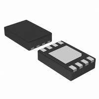
SE97TP,147 NXP Semiconductors, SE97TP,147 Datasheet - Page 18

SE97TP,147
Manufacturer Part Number
SE97TP,147
Description
IC TEMP SENSOR DIMM 8-HWSON
Manufacturer
NXP Semiconductors
Datasheet
1.SE97TK118.pdf
(55 pages)
Specifications of SE97TP,147
Function
Temp Monitoring System (Sensor)
Topology
ADC (Sigma Delta), Comparator, Register Bank
Sensor Type
Internal
Sensing Temperature
-40°C ~ 125°C
Output Type
I²C™/SMBus™
Output Alarm
Yes
Output Fan
Yes
Voltage - Supply
3 V ~ 3.6 V
Operating Temperature
-40°C ~ 125°C
Mounting Type
Surface Mount
Package / Case
8-WSON (Exposed Pad), 8-HWSON
Lead Free Status / RoHS Status
Lead free / RoHS Compliant
Other names
568-4730-2
935286725147
935286725147
NXP Semiconductors
SE97_7
Product data sheet
Fig 16. Page Write timing
SDA
7.10.1.2 Page Write
7.10.1.3 Acknowledge polling
7.10.2 Memory protection
START condition
S
1
slave address (memory)
0
The SE97 contains 256 bytes of data, arranged in 16 pages of 16 bytes each. The page is
selected by the four Most Significant Bits (MSB) of the address byte presented to the
device after the slave address, while the four Least Significant Bits (LSB) point to the byte
within the page. By loading more than one data byte into the device, up to an entire page
can be written in one write cycle (see
increment automatically after each data byte. If the master transmits more than
16 data bytes, then earlier bytes will be overwritten by later bytes in a wrap-around
fashion within the selected page. The internal write cycle is started following the STOP
condition created by the master.
Acknowledge polling can be used to determine if the SE97 is busy writing or is ready to
accept commands. Polling is implemented by sending a ‘Selective Read’ command
(described in
acknowledge the slave address as long as internal write is in progress.
The lower half (the first 128 bytes) of the memory can be write protected by special
EEPROM commands without an external control pin. The SE97 features three types of
memory write protection instructions, and three respective read Protection instructions.
The level of write-protection (set or clear) that has been defined using these instructions
remained defined even after power cycle.
The memory protection commands are:
1
•
•
•
•
•
•
0
Permanent Write Protection (PWP)
Reversible Write Protection (RWP)
Clear Write Protection (CWP)
Read Permanent Write Protection (RPWP)
Read Reversible Write Protection (RRWP)
Read Clear Write Protection (RCWP)
A2 A1 A0
Section 7.10.3 “Read
R/W acknowledge
0
A
from slave
Rev. 07 — 29 January 2010
DDR memory module temp sensor with integrated SPD, 3.3 V
word address
operations”) to the device. The SE97 will not
Figure
acknowledge
from slave
16). The internal byte address counter will
A
write to the memory is performed
data to memory
data to memory
DATA n + 15
DATA n
acknowledge
acknowledge
STOP condition;
from slave
from slave
© NXP B.V. 2010. All rights reserved.
002aab247
A
A
P
SE97
18 of 55


