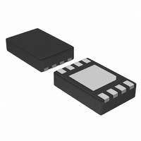
SE97TP,147 NXP Semiconductors, SE97TP,147 Datasheet - Page 27

SE97TP,147
Manufacturer Part Number
SE97TP,147
Description
IC TEMP SENSOR DIMM 8-HWSON
Manufacturer
NXP Semiconductors
Datasheet
1.SE97TK118.pdf
(55 pages)
Specifications of SE97TP,147
Function
Temp Monitoring System (Sensor)
Topology
ADC (Sigma Delta), Comparator, Register Bank
Sensor Type
Internal
Sensing Temperature
-40°C ~ 125°C
Output Type
I²C™/SMBus™
Output Alarm
Yes
Output Fan
Yes
Voltage - Supply
3 V ~ 3.6 V
Operating Temperature
-40°C ~ 125°C
Mounting Type
Surface Mount
Package / Case
8-WSON (Exposed Pad), 8-HWSON
Lead Free Status / RoHS Status
Lead free / RoHS Compliant
Other names
568-4730-2
935286725147
935286725147
NXP Semiconductors
SE97_7
Product data sheet
Table 12.
Bit
7
6
5
4
3
2
1
Symbol
CTLB
AWLB
CEVNT
ESTAT
EOCTL
CVO
EP
Configuration register (address 01h) bit description
Description
Critical Trip Lock bit.
This bit is initially cleared. When set, this bit will return a ‘1’, and remains locked
until cleared by internal Power-on reset. This bit can be written with a single
write and do not require double writes.
Alarm Window Lock bit.
This bit is initially cleared. When set, this bit will return a ‘1’ and remains locked
until cleared by internal power-on reset. This bit can be written with a single write
and does not require double writes.
Clear EVENT (write only).
When read, this register always returns zero.
EVENT Status (read only).
The actual event causing the EVENT can be determined from the Read
Temperature register. Interrupt Events can be cleared by writing to the ‘Clear
EVENT’ bit (CEVNT). Writing to this bit will have no effect.
When either of the Critical Trip or Alarm Window lock bits is set, this bit cannot
be altered until unlocked.
When the Critical Trip or Alarm Window lock bit is set, this bit cannot be altered
until unlocked.
EVENT Polarity.
EVENT Output Control.
Critical Event Only.
•
0 — Critical Alarm Trip register is not locked and can be altered (default)
1 — Critical Alarm Trip register settings cannot be altered
0 — Upper and Lower Alarm Trip registers are not locked and can be altered
(default)
1 — Upper and Lower Alarm Trip registers setting cannot be altered
0 — no effect (default)
1 — clears active EVENT in Interrupt mode. Writing to this register has no
effect in Comparator mode.
0 — EVENT output condition is not being asserted by this device (default)
1 — EVENT output pin is being asserted by this device due to Alarm Window
or Critical Trip condition
0 — EVENT output disabled (default)
1 — EVENT output enabled
0 — EVENT output on Alarm or Critical temperature event (default)
1 — EVENT only if temperature is above the value in the critical temperature
register
0 — active LOW (default)
1 — active HIGH. When either of the Critical Trip or Alarm Window lock bits is
set, this bit cannot be altered until unlocked.
Advisory note:
– JEDEC specification requires only the Alarm Window lock bit to be set.
– Work-around: Clear both Critical Trip and Alarm Window lock bits.
– Future 1.7 V to 3.6 V SE97B will require only the Alarm Window lock bit
Rev. 07 — 29 January 2010
to be set.
DDR memory module temp sensor with integrated SPD, 3.3 V
…continued
© NXP B.V. 2010. All rights reserved.
SE97
27 of 55


