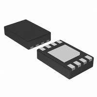
SE97TP,147 NXP Semiconductors, SE97TP,147 Datasheet - Page 39

SE97TP,147
Manufacturer Part Number
SE97TP,147
Description
IC TEMP SENSOR DIMM 8-HWSON
Manufacturer
NXP Semiconductors
Datasheet
1.SE97TK118.pdf
(55 pages)
Specifications of SE97TP,147
Function
Temp Monitoring System (Sensor)
Topology
ADC (Sigma Delta), Comparator, Register Bank
Sensor Type
Internal
Sensing Temperature
-40°C ~ 125°C
Output Type
I²C™/SMBus™
Output Alarm
Yes
Output Fan
Yes
Voltage - Supply
3 V ~ 3.6 V
Operating Temperature
-40°C ~ 125°C
Mounting Type
Surface Mount
Package / Case
8-WSON (Exposed Pad), 8-HWSON
Lead Free Status / RoHS Status
Lead free / RoHS Compliant
Other names
568-4730-2
935286725147
935286725147
NXP Semiconductors
Table 29.
V
[1]
SE97_7
Product data sheet
Symbol
I
I
V
V
V
V
V
V
I
I
I
I
I
C
I
I
Z
Z
DD(AV)
sd(VDD)
OL(sink)EVENT
OL(sink)(SDA)
LOH
LIH
LIL
L
pd
DD
IL
IH
IH
IL
OL1
OL2
I(ov)
POR
i(SCL/SDA)
= 1.7 V to 3.6 V; T
High-voltage input voltage applied to pin A0 during RWP and CRWP operations. The JEDEC specification is 7 V (min.) and 10 V (max.),
but since the SE97 EEPROM write works only down to 3.0 V, the condition of V
minimum voltage changed to 7.8 V. If V
DC characteristics
Parameter
average supply current
supply voltage shutdown mode
current
HIGH-level input voltage
LOW-level input voltage
LOW-level output voltage 1
LOW-level output voltage 2
overvoltage input voltage
power-on reset voltage
LOW-level output sink current on
pin EVENT
LOW-level output sink current on
pin SDA
HIGH-level output leakage current
HIGH-level input leakage current
LOW-level input leakage current
SCL and SDA input capacitance
leakage current
pull-down current
LOW-level input impedance
HIGH-level input impedance
amb
=
−
40
°
C to +125
DD
is 3.6 V then the minimum voltage is 8.4 V.
°
C; unless otherwise specified. These specifications are guaranteed by design.
Rev. 07 — 29 January 2010
DDR memory module temp sensor with integrated SPD, 3.3 V
Conditions
SMBus inactive
SMBus inactive
SCL, SDA;
V
SCL, SDA;
V
V
V
pin A0; V
power supply rising
power supply falling
V
V
EVENT; V
SDA, SCL; V
SDA, SCL; V
A0, A1, A2; V
on A0, A1, A2
internal; A0, A1, A2 pins;
V
pins A0, A1, A2; V
pins A0, A1, A2
DD
DD
DD
DD
OL1
OL2
I
SE97PW, SE97TK
SE97TL, SE97TP
SE97PW, SE97TK
SE97TL, SE97TP
= 0.3V
= 3.0 V to 3.6 V
= 3.0 V to 3.6 V
= 3.0 V; I
= 1.7 V; I
= 0.4 V
= 0.5 V
I(ov)
DD
OH
to V
I
I
− V
= V
OL
OL
I
= V
= V
= V
DD
= 3 mA
= 1.5 mA
DD
DD
DD
SS
SS
I
< 0.3V
> 4.8 V
I(ov)
> 4.8 V + V
DD
[1]
Min
-
-
0.7 × V
-
-
-
7.8
-
0.1
0.6
2
6
3
−1.0
−1.0
−1.0
−1.0
-
-
-
30
800
DD
or > 4.8 V + 3.0 V was applied and the
DD
Typ
250
0.1
-
-
-
-
-
-
-
-
-
-
-
-
-
-
-
5
1
-
-
-
© NXP B.V. 2010. All rights reserved.
400
1.7
-
10
Max
5.0
V
0.3 × V
0.4
0.5
10
-
-
-
-
+1.0
+1.0
+1.0
+1.0
-
4.0
-
-
DD
+ 1
SE97
DD
39 of 55
Unit
μA
μA
V
V
V
V
V
V
V
V
mA
mA
mA
μA
μA
μA
μA
pF
μA
μA
kΩ
kΩ


