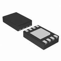
SE97TP,147 NXP Semiconductors, SE97TP,147 Datasheet - Page 19

SE97TP,147
Manufacturer Part Number
SE97TP,147
Description
IC TEMP SENSOR DIMM 8-HWSON
Manufacturer
NXP Semiconductors
Datasheet
1.SE97TK118.pdf
(55 pages)
Specifications of SE97TP,147
Function
Temp Monitoring System (Sensor)
Topology
ADC (Sigma Delta), Comparator, Register Bank
Sensor Type
Internal
Sensing Temperature
-40°C ~ 125°C
Output Type
I²C™/SMBus™
Output Alarm
Yes
Output Fan
Yes
Voltage - Supply
3 V ~ 3.6 V
Operating Temperature
-40°C ~ 125°C
Mounting Type
Surface Mount
Package / Case
8-WSON (Exposed Pad), 8-HWSON
Lead Free Status / RoHS Status
Lead free / RoHS Compliant
Other names
568-4730-2
935286725147
935286725147
NXP Semiconductors
Table 5.
[1]
[2]
[3]
SE97_7
Product data sheet
Command
Normal EEPROM read/write
Reversible Write Protection (RWP)
Clear Reversible Write Protection (CRWP)
Permanent Write Protection (PWP)
Read RWP
Read CRWP
Read PWP
Fig 17. Software Write Protect (write)
The most significant bit, bit 7, is sent first.
A0, A1, and A2 are compared against the respective external pins on the SE97.
V
I(ov)
(1) Refer to
ranges from 7.8 V to 10 V.
SDA
X = Don’t Care
EEPROM commands summary
START condition
S
Table 6
0
slave address (memory)
1
Table 5
This special EEPROM command consists of a unique 4-bit fixed address (0110b) and the
voltage level applied on the 3-bit hardware address. Normally, to address the memory
array, the 4-bit fixed address is ‘1010b’. To access the memory protection settings, the
4-bit fixed address is ‘0110b’.
sequence, respectively.
Up to eight memory devices can be connected on a single I
3-bit on the hardware selectable address (A2, A1, A0) inputs. The device only responds
when the 4-bit fixed and hardware selectable bits are matched. The 8th bit is the
read/write bit. This bit is set to 1 or 0 for read and write protection, respectively.
The corresponding device acknowledges during the ninth bit time when there is a match
on the 7-bit address.
The device does not acknowledge when there is no match on the 7-bit address or when
the device is already in permanent write protection mode and is programmed with any
write protection instructions (i.e., PWP, RWP, CWP).
regarding the exact state of the acknowledge bit.
1
0
A2 A1 A0
is the summary for normal and memory protection instructions.
[2]
R/W acknowledge
0
A
from slave
Fixed address
Bit 7
1
0
0
0
0
0
0
Rev. 07 — 29 January 2010
X
DDR memory module temp sensor with integrated SPD, 3.3 V
[1]
X
dummy byte address
Bit 6
0
1
1
1
1
1
1
X
(1)
Figure 17
X
X
Bit 5
1
1
1
1
1
1
1
acknowledge
X
and
X
from slave
Figure 18
X
Bit 4
0
0
0
0
0
0
0
(1)
A
X
X
show the write and read protection
Hardware selectable
address
Bit 3
A2
V
V
A2
V
V
A2
SS
SS
SS
SS
X
dummy data
2
X
C-bus. Each one is given a
X
Bit 2
A1
V
V
A1
V
V
A1
SS
DD
SS
DD
acknowledge
X
STOP condition
X
from slave
© NXP B.V. 2010. All rights reserved.
Bit 1
A0
V
V
A0
V
V
A0
X
002aab356
I(ov)
I(ov)
I(ov)
I(ov)
(1)
A
[3]
[3]
[3]
[3]
P
SE97
R/W
Bit 0
R/W
0
0
0
1
1
1
19 of 55


