ISL8120IRZ-T Intersil, ISL8120IRZ-T Datasheet - Page 28
ISL8120IRZ-T
Manufacturer Part Number
ISL8120IRZ-T
Description
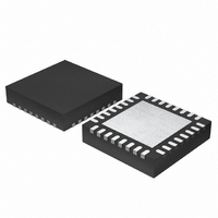
IC CTRLR PWM 2/NPHASE 32-QFN
Manufacturer
Intersil
Datasheet
1.ISL8120IRZ-T.pdf
(33 pages)
Specifications of ISL8120IRZ-T
Pwm Type
Voltage Mode
Number Of Outputs
2
Frequency - Max
1.5MHz
Duty Cycle
90%
Voltage - Supply
3 V ~ 22 V
Buck
Yes
Boost
No
Flyback
No
Inverting
No
Doubler
No
Divider
No
Cuk
No
Isolated
No
Operating Temperature
-40°C ~ 85°C
Package / Case
32-VQFN Exposed Pad, 32-HVQFN, 32-SQFN, 32-DHVQFN
Frequency-max
1.5MHz
Lead Free Status / RoHS Status
Lead free / RoHS Compliant
Available stocks
Company
Part Number
Manufacturer
Quantity
Price

Part Number:
ISL8120IRZ-T
Manufacturer:
INTERSIL
Quantity:
20 000


The reason of which is practical especially for low DCR
applications the PCB and inductor pad soldering resistance
would have large effects in total impedance affecting the
DCR voltage to be sensed.
When OCP is triggered, the controller pulls EN/FF low
immediately to turn off UGATE and LGATE. However, if the
output overshoot is greater than 113% at EN/FF = LOW,
LGATE turns ON until the output voltage drops below 87%.
A delay time, equal to 3 soft-start intervals, is entered to
allow the disturbance to clear. After the delay time, the
controller then initiates a soft-start interval. If the output
voltage comes up and returns to the regulation, PGOOD
transitions high. If the OC trip is exceeded during the
soft-start interval, the controller pulls EN/VFF low again. The
PGOOD signal will remain low and the soft-start interval will
be allowed to expire. Another soft-start interval will be
initiated after the delay interval. If an overcurrent trip occurs
again, this same cycle repeats until the fault is removed.
There is a100ns delay to prevent any fault triggering during
start-up or load transient. For a hard short of the output, the
overcurrent protection reduces the regulator RMS output
current much less than 60% of the full load current by putting
the controller into hiccup mode.
Internal Series Linear and Power Dissipation
The VIN pin is connected to PVCC with an internal series
linear regulator (1W Typical), which is internally
compensated. The PVCC and VIN pins should have the
recommended bypasses connected to GND for proper
operation. The internal series linear regulator’s input (VIN)
can range between 3V to 22V. The internal linear regulator is
to provide power for both the internal MOSFET drivers
through the PVCC pin and the analog circuitry through the
VCC pin. The VCC pin should be connected to the PVCC pin
with an RC filter to prevent high frequency driver switching
noise from entering the analog circuitry. When VIN drops
below 5.0V, the pass element will saturate; PVCC will track
VIN, minus the dropout of the linear regulator. When used
with an external 5V supply, VIN pin is recommended to be
tied directly to PVCC.
28
ISL8120IRZEC
The LDO is capable to supply 250mA with regulated 5.4V
output. In 3.3V input applications, when the VIN pin voltage
is 3V, the LDO still can supply 150mA while maintaining LDO
output voltage higher than VCC falling threshold to keep IC
operating. Figure 17 shows the LDO voltage drop under
different load current. However, its thermal capability should
not be exceeded. The power dissipation inside the IC could
be estimated with Equation 7.
P
I
VIN
IC
FIGURE 16. INTERNAL REGULATOR IMPLEMENTATION
1µF
=
6.0
5.5
5.0
4.5
4.0
3.5
3.0
2.5
2.0
=
(
2.5
VIN PVCC
⎛
⎜
⎝
5V
Q
----------------------------- -
G1
VCC
Z1
V
PVCC @ 250mA + Iq
–
2Ω
3.0
FIGURE 17. PVCC vs VIN VOLTAGE
GS1
•
N
Q1
3.5
Z2
) I
+
PVCC
⋅
2.65V TO 5.6V
Q
----------------------------- -
VIN
G2
4.0
VIN PIN VOLTAGE (V)
V
PVCC @ 140mA + Iq
GS2
+
•
Iq IS AROUND 15mA
N
P
4.5
Q2
DR
⎞
⎟
⎠
•
10µF
PVCC @ 100mA + Iq
5.0
PVCC F
5.5
3V TO 26.4V
•
SW
6.0
+
I
Q_VIN
6.5
April 21, 2009
VIN
(EQ. 7)
FN6763.1
7.0
Related parts for ISL8120IRZ-T
Image
Part Number
Description
Manufacturer
Datasheet
Request
R

Part Number:
Description:
Dual/n-phase Buck Pwm Controller With Integrated Drivers
Manufacturer:
Intersil Corporation
Datasheet:
Part Number:
Description:
Intersil Corporation [CMOS Serial Controller Interface]
Manufacturer:
Intersil Corporation
Datasheet:
Part Number:
Description:
Manufacturer:
Intersil Corporation
Datasheet:
Part Number:
Description:
357-036-542-201 CARDEDGE 36POS DL .156 BLK LOPRO
Manufacturer:
Intersil Corporation
Datasheet:
Part Number:
Description:
1024-Word x 4-Bit LSI Static RAM
Manufacturer:
Intersil Corporation
Datasheet:
Part Number:
Description:
General Purpose NPN Transistor Arrays FN341.4
Manufacturer:
Intersil Corporation
Datasheet:
Part Number:
Description:
CMOS 16-Bit Microprocessor
Manufacturer:
Intersil Corporation
Datasheet:
Part Number:
Description:
Manufacturer:
Intersil Corporation
Datasheet:
Part Number:
Description:
Manufacturer:
Intersil Corporation
Datasheet:
Part Number:
Description:
Manufacturer:
Intersil Corporation
Datasheet:
Part Number:
Description:
Manufacturer:
Intersil Corporation
Datasheet:
Part Number:
Description:
CMOS 6-Bit Latch and Decoder Memory Interfaces
Manufacturer:
Intersil Corporation
Datasheet:
Part Number:
Description:
CA3046General Purpose NPN Transistor Arrays
Manufacturer:
Intersil Corporation
Datasheet:
Part Number:
Description:
Manufacturer:
Intersil Corporation
Datasheet:
Part Number:
Description:
TR909 DLC/FLC SLIC with Low Power Standby
Manufacturer:
Intersil Corporation
Datasheet: