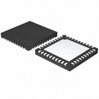
ISL6260CRZ Intersil, ISL6260CRZ Datasheet - Page 21

ISL6260CRZ
Manufacturer Part Number
ISL6260CRZ
Description
IC CORE REG MULTIPHASE 40-QFN
Manufacturer
Intersil
Datasheet
1.ISL6260BCRZ.pdf
(26 pages)
Specifications of ISL6260CRZ
Applications
Converter, Intel IMVP-6
Number Of Outputs
1
Voltage - Output
0.3 ~ 1.5 V
Operating Temperature
-10°C ~ 100°C
Mounting Type
Surface Mount
Package / Case
40-VFQFN, 40-VFQFPN
Lead Free Status / RoHS Status
Lead free / RoHS Compliant
Voltage - Input
-
Available stocks
Company
Part Number
Manufacturer
Quantity
Price
Company:
Part Number:
ISL6260CRZ
Manufacturer:
Intersil
Quantity:
74
Part Number:
ISL6260CRZ
Manufacturer:
INTERSIL
Quantity:
20 000
Part Number:
ISL6260CRZ-T
Manufacturer:
INTERSIL
Quantity:
20 000
Static Mode of Operation - Static Droop using DCR
Sensing
As previously mentioned, the ISL6260 and ISL6260B have
an internal differential amplifier which provides for extremely
accurate voltage regulation at the die of the processor. The
load line regulation is also very accurate, and the process of
selecting the components for the appropriate load line droop
is explained here.
For DCR sensing, the process of compensation for DCR
resistance variation to achieve the desired load line droop
has several steps and is somewhat iterative. Refer to
Figure 42.
In Figure 42 we show a 3 phase solution using DCR
sensing. There are two resistors around the inductor of each
phase. These are labeled RS and RO. These resistors are
used to arrive at the DC voltage drop across each inductor.
Each inductor will have a certain level of DC current flowing
through it, this current when multiplied by the DCR of the
inductor creates a small DC level of voltage. When this
voltage is summed with the other channels DC voltages, the
total DC load current can be derived.
RO is typically 5 to 10Ω. This resistor is used to tie the
outputs of all channels together and thus create a summed
average of the local CORE voltage output. RS is determined
through an understanding of both the DC and transient load
currents. This value will be covered in the next section.
However, it is important to keep in mind that the output of
each of these RS resistors are tied together to create the
VSUM voltage node. With both the outputs of RO and RS
tied together, the simplified model for the droop circuit can
be derived. This is presented in Figure 43.
IS E N 1
O C
In te r n a l to
IS L 6 2 6 0
V D IF F
IS E N 1
0 .2 2 u F
Σ
-
+
+
+
IS E N 2
1 0 u A
R o p n 2
R T N
1
1
+
+
-
-
FIGURE 42. EQUIVALENT MODEL FOR DROOP AND DIE SENSING USING DCR SENSING
IS E N 2
0 .0 1 u F
21
D R O O P
V S E N
IS E N 3
-
+
D R O O P
O C S E T
V S U M
1 0
D F B
V C C _ S E N S E
IS E N 3
V S S _ S E N S E
R o p n 1
V O '
R
O C S E T
to V o u t
ISL6260, ISL6260B
T o P r o c e s s o r
S o c k e t K e lv in
C o n n e c tio n s
V O '
V S U M
V O '
Figure 43 shows the simplified model of the droop circuitry.
Essentially one resistor can replace the RO resistors of each
phase and one RS resistor can replace the RS resistors of
each phase. The total DCR drop due to load current can be
replaced by a DC source, the value of which is given by
Equation 5.
where N is the number of channels designed for Active
operation. N = 3 for this example. Another simplification can
be done by reducing the NTC network comprised of Rntc,
Rseries and Rparallel, given in Figure 43, to a single resistor
given as Rn.
The first step in droop load line compensation is to adjust
Rn, RO
exists even at light loads between the VSUM and VO’ nodes.
We recognize that these components form a voltage divider.
As a rule of thumb we start with the voltage drop across the
Rn network, VN, to be 0.57 x Vdcr. This ratio provides for a
fairly reasonable amount of light load signal from which to
arrive at droop.
First we calculate the equivalent NTC network resistance,
Rn. Typical values that provide good performance are,
Rseries = 3.57K_1%, Rpar = 4.53K_1% and Rntc = 10kΩ
NTC, ERT-J1VR103J from Panasonic. Rn is then given by
Equation 6.
In our second step we calculate the series resistance from
each phase to the Vsum node, labeled RS1, RS2 and RS3
in Figure 42.
Rn
Vdcr
=
V S U M
V S U M
V S U M
EQV
(
--------------------------------------------------------------------
Rseries
Rseries
EQV
I
p h a s e 1
I
p h a s e 2
=
I
p h a s e 3
R S 1
R S 2
R S 3
Iout
------------------------------ -
and RS
+
+
×
Rntc
Rntc
N
DCR
EQV
IS E N 2
IS E N 3
IS E N 1
)
+
R
R
×
Rpar
L
L 2
L 3
R
L
Rpar
such that sufficient droop voltage
2
L 1
3
L
1
=
+
V O '
+
V d c r
C
C
3.4kΩ
C
V d c r
V O '
D C R
L 2
L 3
L 1
+
V O '
2
-
V d c r
D C R
3
D C R
-
R O 1
1
-
R O 3
R O 2
E S R
V o u t
January 3, 2006
C
b u lk
(EQ. 6)
FN9162.1
(EQ. 5)


